ENGR338 Lab 2021
Spring
Lab 2 Design an R-2R DAC
Name: Sean
Eaton
Email:
smeaton@fortlewis.edu
Design an
R-2R DAC
Introduction
In this lab we will be using Electric VLSI and LTSpice in order to
understand the operation of the ideal analog to digital convertor (ADC)
and the ideal digital to analog convertor (DAC). Then we will be
replacing the ideal DAC with the R-2R DAC we will be creating in
Electric VLSI.
Task 1:
The Electric VLSI and LTSpice configuration setup should be done prior
to task 1. If not the Electric VLSI tutorial 1 should be completed.
Next the libraries of the ideal ADC and DAC should be downloaded and a
new library called ENGR338 should be created.
In Electric VLSI, navigate to Cell < Cross-Library Copy and copy
sim_ADC_DAC{sch} making sure that the Copy subcells and the Copy all
related views boxes are checked. This is so only that particular file
needs to be copied and all the other files are automatically copied.
Now the sim_ADC_DAC{sch} schematic should be opened. Run the LTSpice
simulation by navigating to Tools > Simulation (Spice) >
Write Spice Deck. The schematic is shown in Figure 1 below. Verify that
the simulation plotting matches the one shown below in Figure 2 as well.
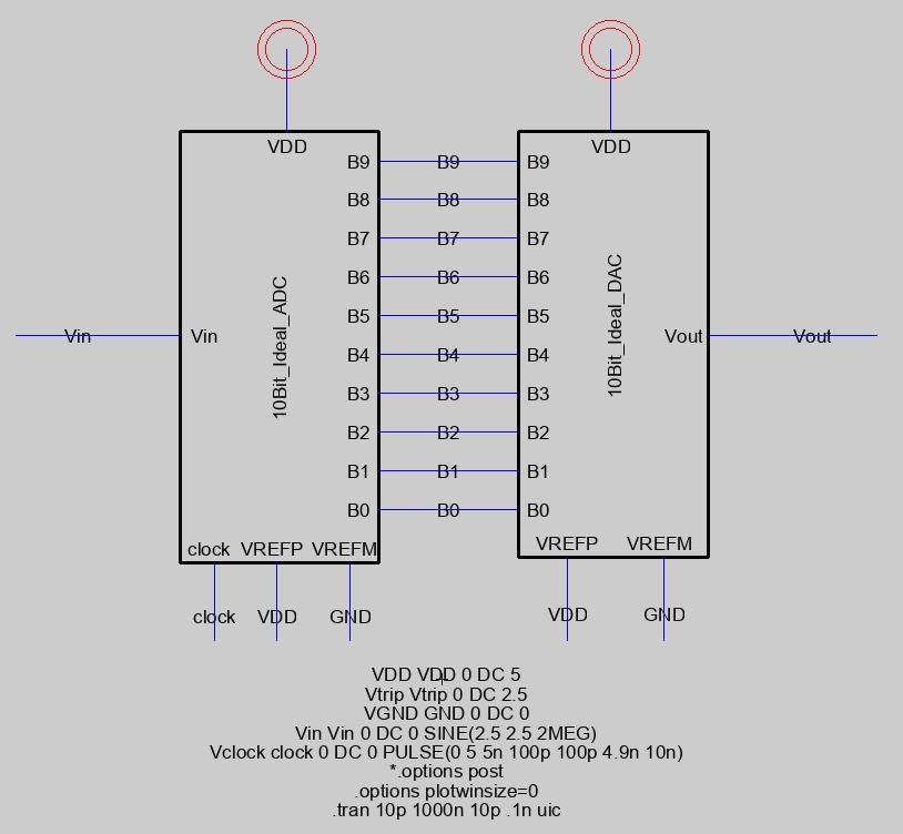 Figure 1. The schematic for the ideal ADC to ideal DAC simulation.
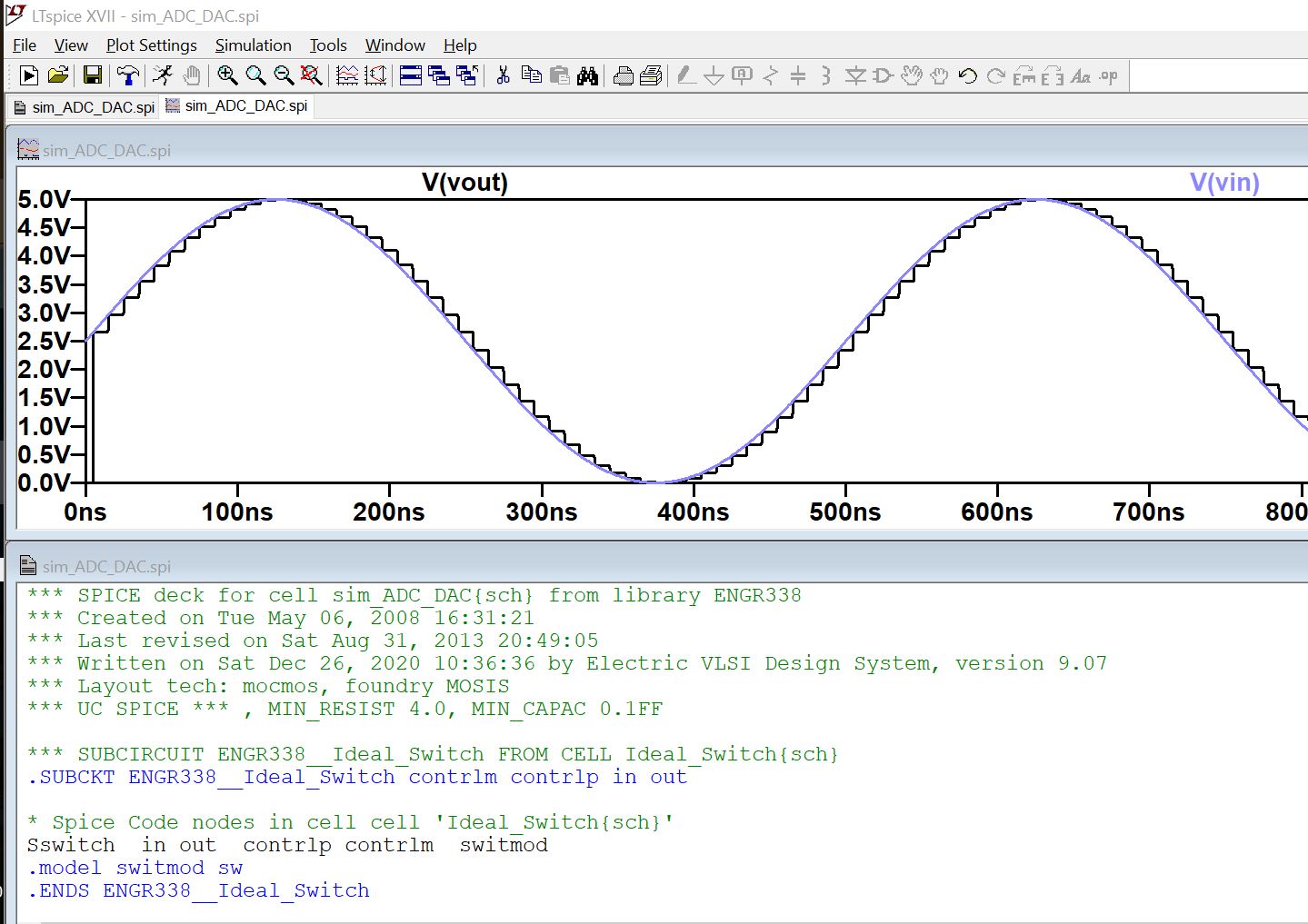 Figure 2. Reference simulation results for the ADC to DAC schematic.
Task 2:
In task 2 we were tasked with creating the 10-bit R-2R ladder schematic
in Electric VLSI and confirming that the DRC Check passes with no
errors or warnings. The schematic should like the one shown below in
Figure 3.
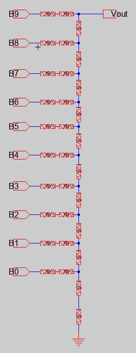 Figure 3. The 10-bit R-2R Electric VLSI schematic.
Then an icon view should be created for the schematic. Using the icon
of the schematic, replace the ideal DAC in the ideal ADC to ideal DAC
simulation schematic with the R-2R Ladder icon. After
replacing the ideal DAC with the R-2R ladder reconnect the appropriate
bits together and name the output arc to Vout so LTSpice can recognize
it. The result should look similar to Figure 4 below.
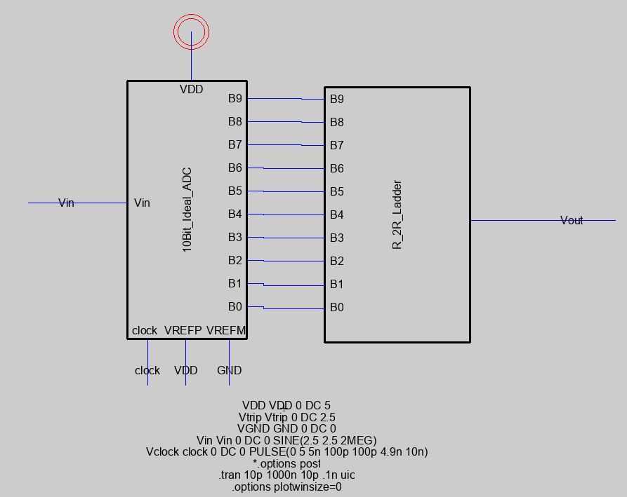 Figure 4. Simulation schematic for the ideal ADC to our R-2R Ladder
icon.
Figure 4. Simulation schematic for the ideal ADC to our R-2R Ladder
icon.
Now run the simulation. The results should be very similar to the ideal
ADC and ideal DAC simulation shown in Figure 2 previously.
Task 3:
In task 3 we
had to calculate the time delay for the B9 pin when the R-2R DAC output
was driving a 10 pF capacitor load. In order to measure the time delay
for the B9 pin the pins B0 to B8 should all be grounded and a capacitor
added as shown below in Figure 5.
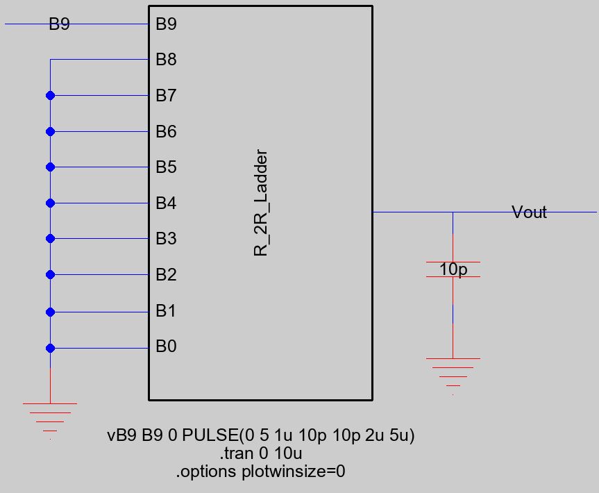 Figure 5. The simulation schematic for task 3.
The
Thevenin's equivalent circuit was also provided as shown in Figure 6.
The time delay should be calculated and compared to the measured
simulation results.
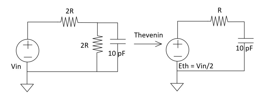 Figure 6. The Thevenin's equivalent circuit for the R-2R ladder configuration for Task 3.
Results
Task 1: In task 1 the Lab 2 library was successfully copied over to the
ENGR338 library I created. I then opened the sim_ADC_DAC{sch} and ran a
DRC check for errors.
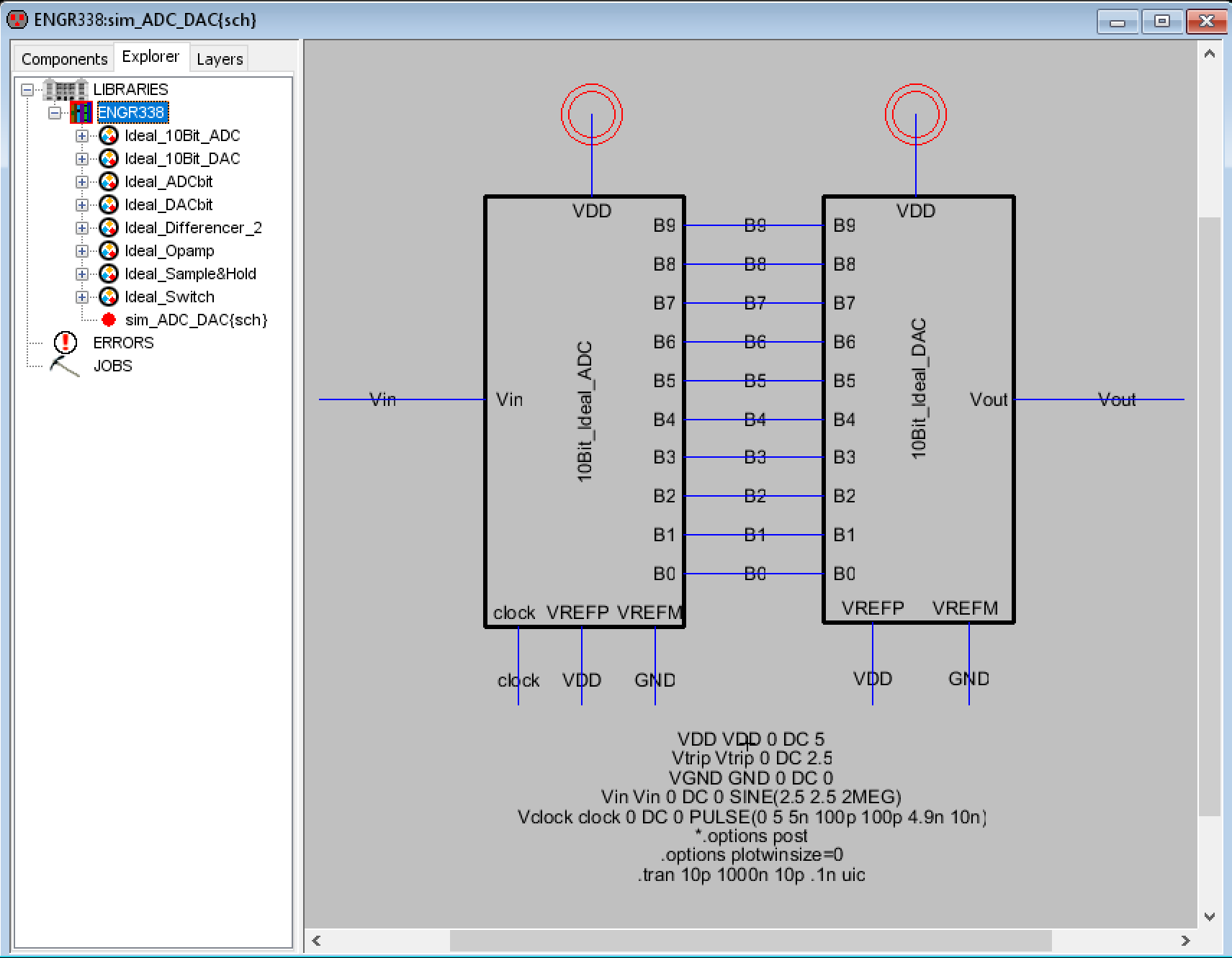
Figure 7. Viewing the sim_ADC_DAC{sch} from the ENGR338 library.
The
DRC check resulted in two warnings but no errors as shown below in
Figure 8. The simulation was successful after writing the spice deck
however as shown below in Figure 9.
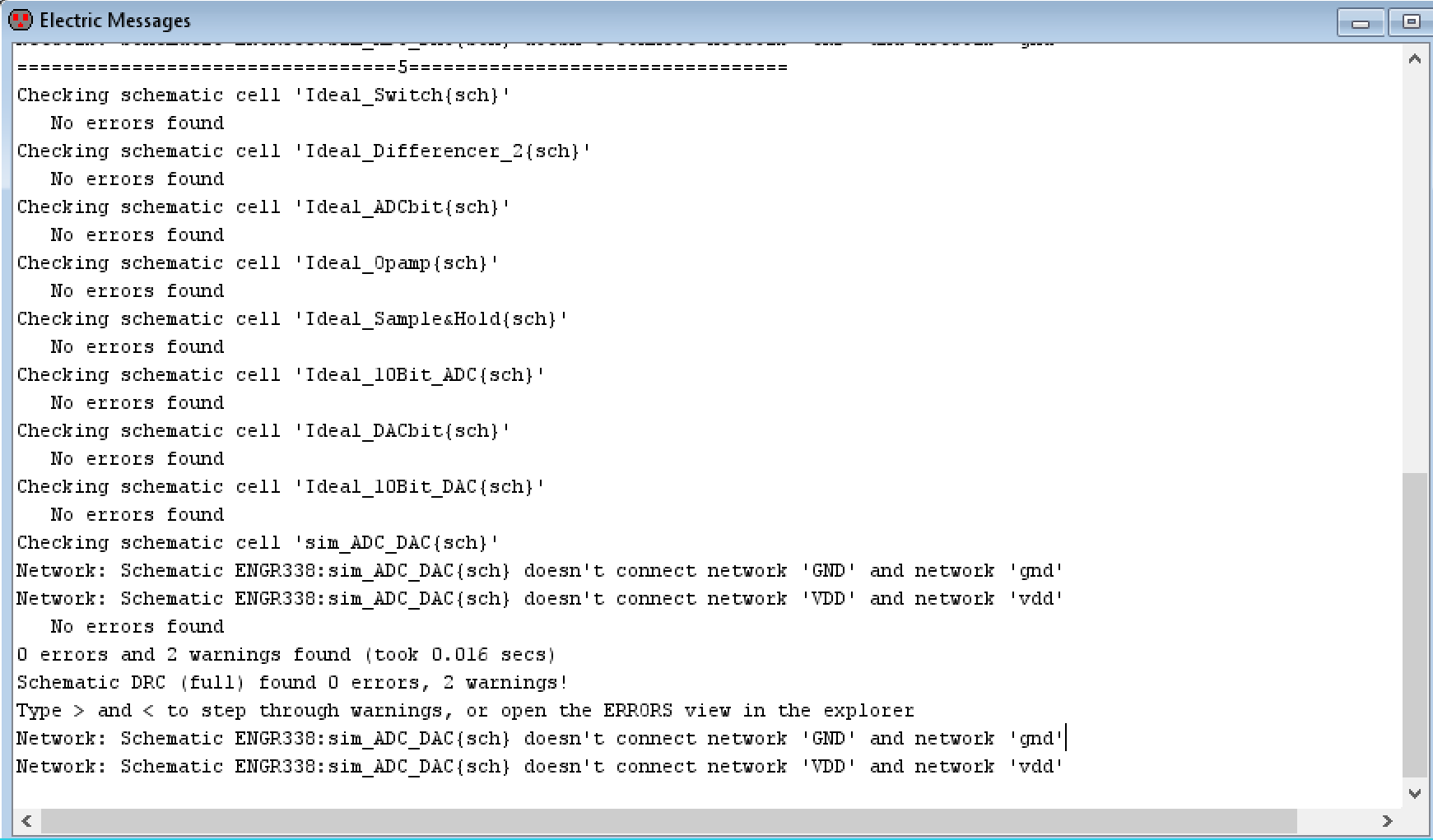 Figure 8. DRC Check results, no errors were found but there were two warnings.
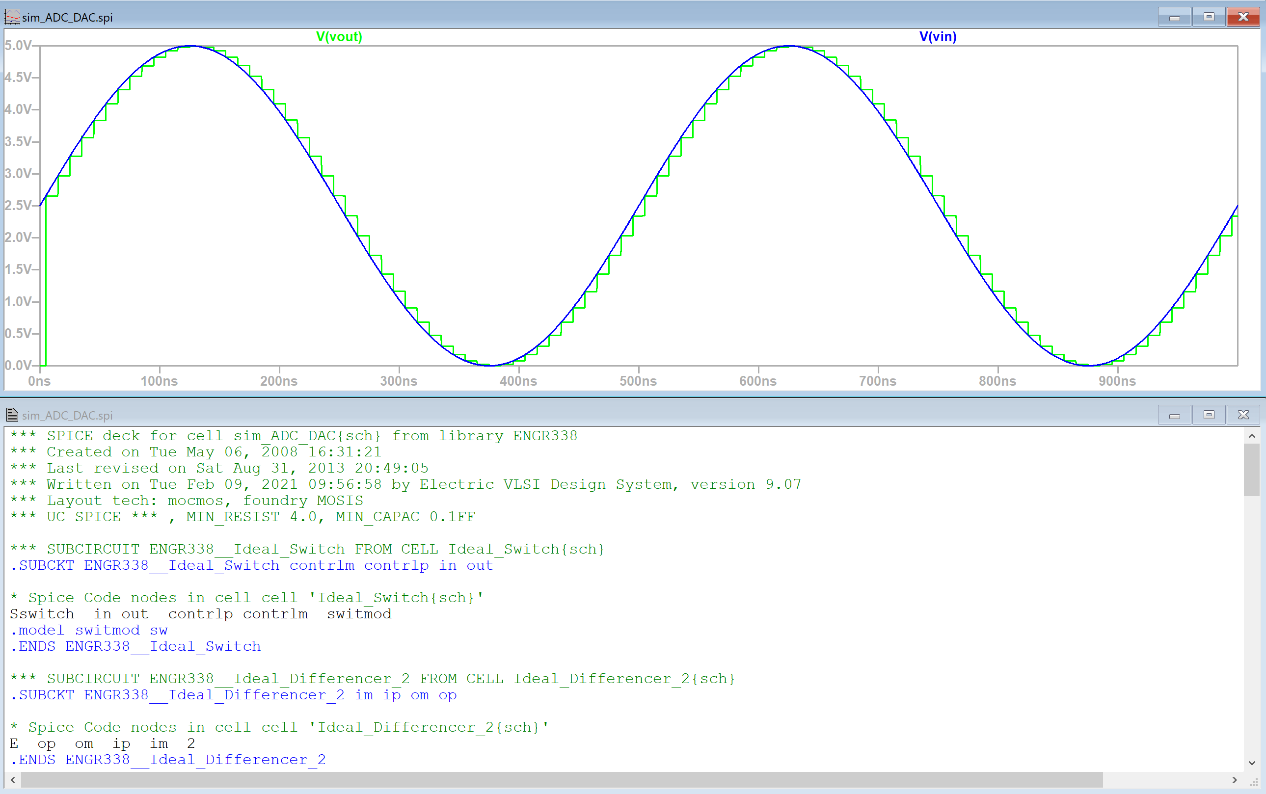 Figure 9. LTSpice simulation results for the ideal ADC to ideal DAC schematic.
Task
2: The R-2R Ladder was successfully implemented in the schematic view
as shown below in Figure 10. Resistor values were 10k and the ports
were exported appropriately.
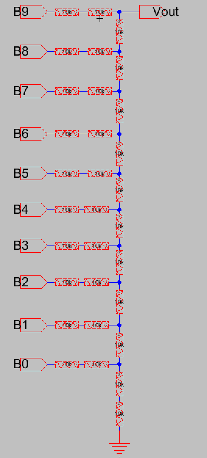
Figure 10. Schematic view of the R-2R Ladder DAC.
After
implementing the R-2R Ladder in the schematic view, a DRC check was ran
and the icon view was created. Text was added to the icon so that pin
names could be seen after connecting the R-2R Ladder to the ideal ADC.
Figure 11 shows the results of the DRC check and Figure 12 displays the
finished icon.
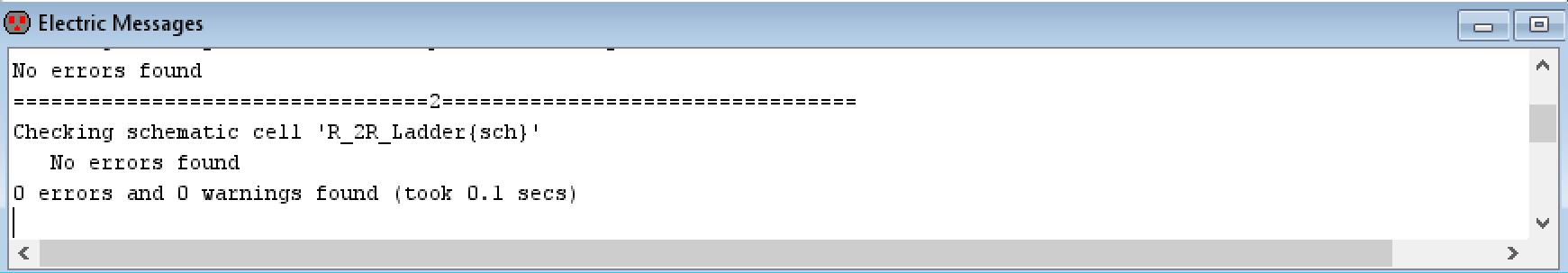
Figure 11. DRC Check results for the R-2R Ladder schematic.
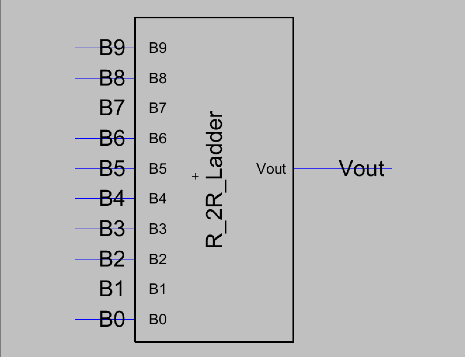
Figure 12. Icon view of the R-2R Ladder DAC.
Next
the R-2R Ladder DAC icon was used in a copy of the simulation used in
Task 1, it was renamed to sim_ADC_R_2R_DAC{sch}. Figure 13 shows the
R-2R Ladder DAC connected to the ideal ADC.
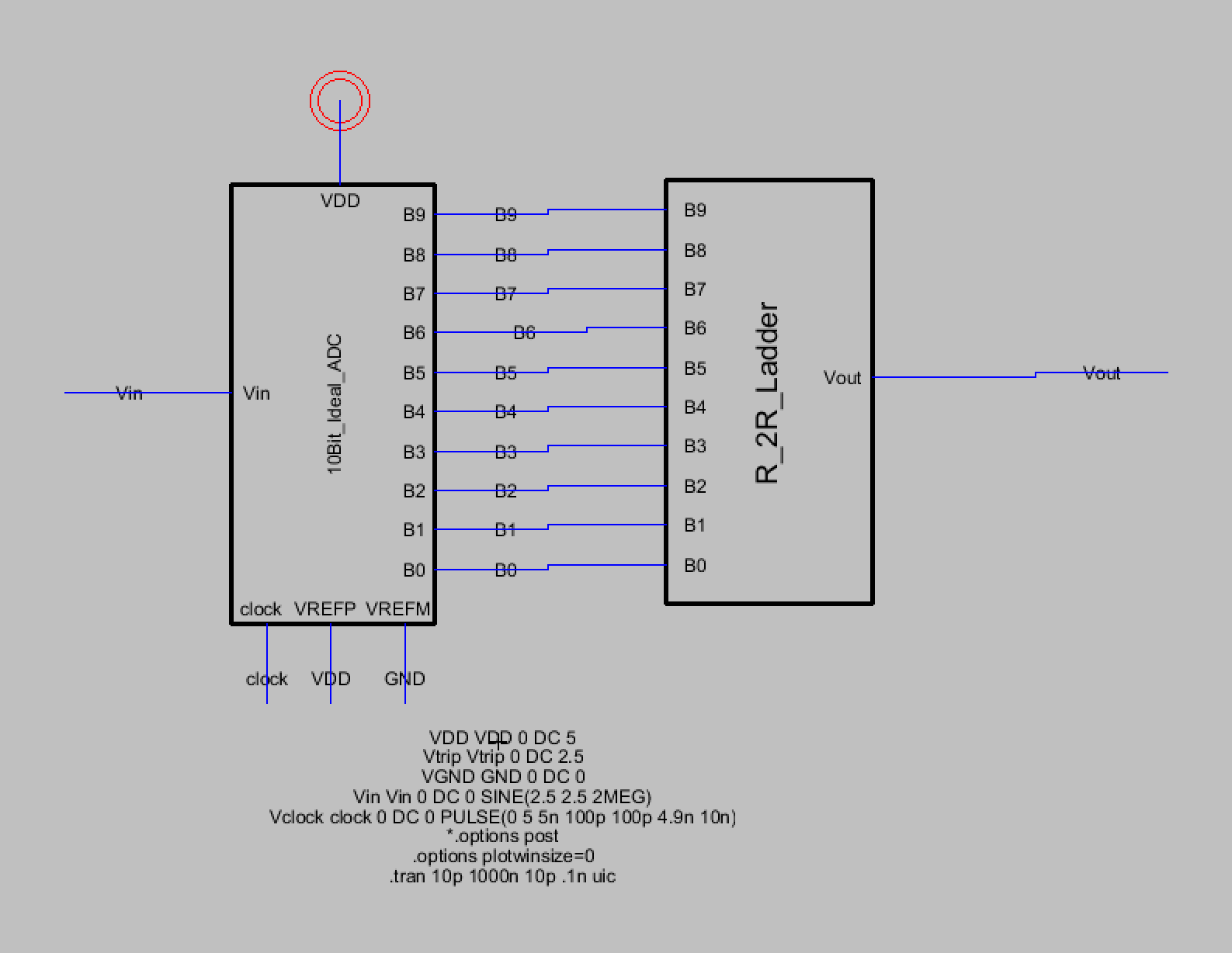
Figure 13. Ideal ADC to R-2R Ladder DAC simulation schematic.
Then
the schematic was simulated using LTSpice, the results are shown below
in Figure 14. The results are very similar to the ideal DAC used in
Task 1.
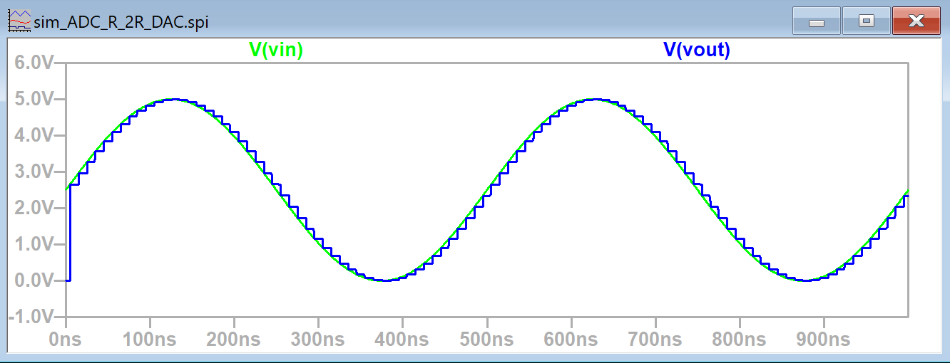
Figure 14. LTSpice simulation of the ideal ADC to 2-2R Ladder DAC.
Task
3: In task 3 the time delay was successfully calculated and measured.
First the simulation schematic used in task 2 was duplicated for the
time delay test. The ideal ADC was deleted so that only the R-2R Ladder
DAC was in the schematic. Next pins B8 to B0 were grounded and spice
code defining B9 as a PULSE function was added. Then a 10 pF capacitor
load was added to Vout.
The resulting schematic is shown in Figure 15.
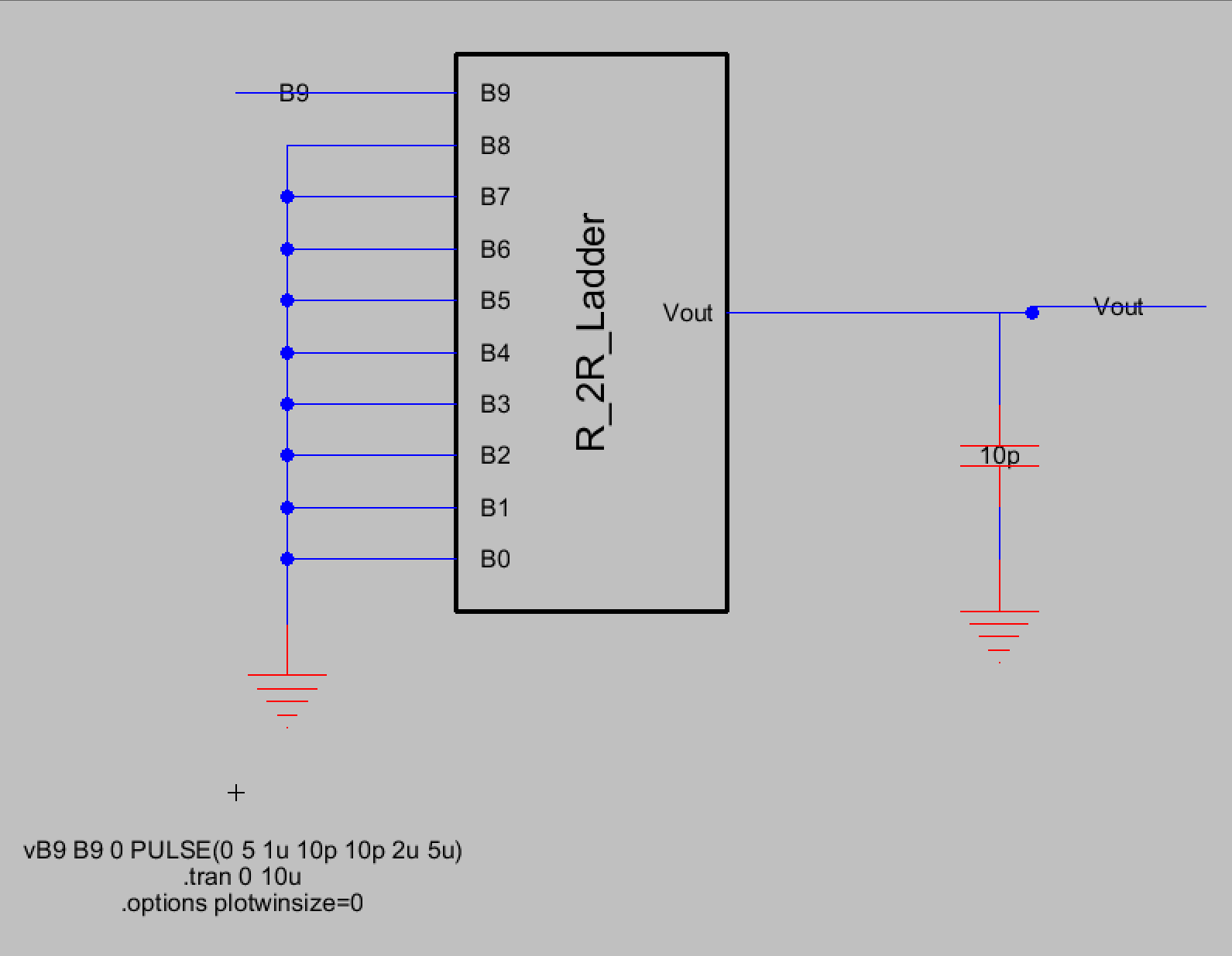
Figure 15. Simulation schematic for testing the time delay of the R-2R Ladder DAC with a 10 pF load
The
Thevenin's equivalent circuit was provided to us and is shown below in
Figure 16. The Thevenin's equivalent voltage was found to be one half
of the voltage input. Since the PULSE function is providing 5V when
high, this would mean that the Thevenin's equivalent voltage at the
maximum would be 2.5V. The Thevenin's equivalent resistance was found
to be R or 10k ohms. The Thevenin's equivalent circuit is shown below
in Figure 16.
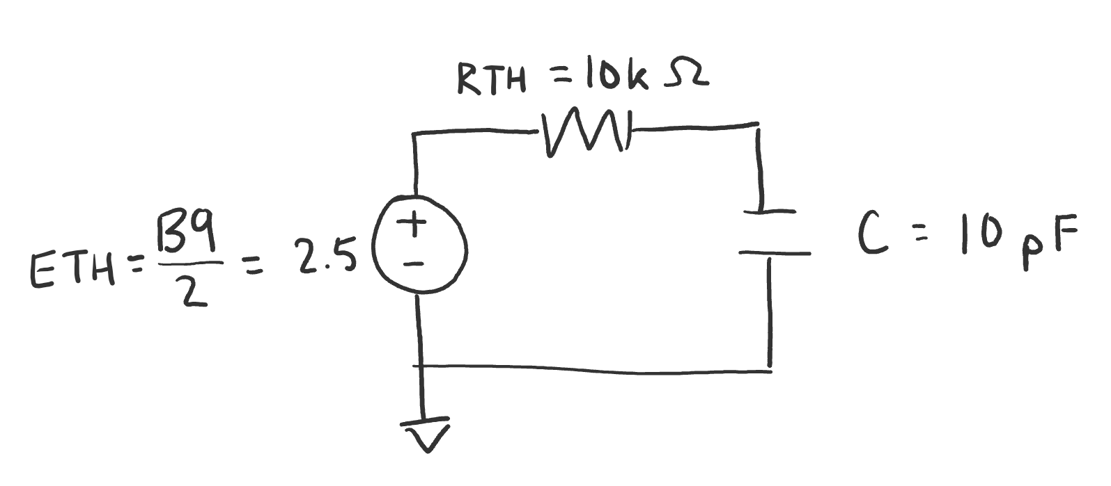
Figure 16. The Thevenin's equivalent circuit for task 3.
The time delay was calculated as shown in Figure 17. It was found that it should be 70 ns.
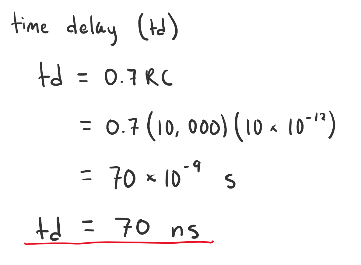
Figure 17. Calculating time delay using 0.7RC.
The
circuit was then simulated to measure the time delay. Since the
Thevenin's equivalent voltage was 2.5V this meant that the halfway
point would be 1.25V even though the voltage input at B9 was 5V. It was
then confirmed that the time delay is indeed 70 ns. Figure 18 shows
that the time difference is a little above 70 ns but this is due to the
difficult in getting the cursor to be exactly at 1.25V.
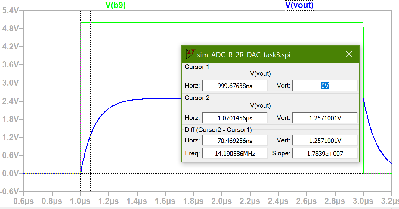
Figure 18. Measuring time delay in the LTSpice simulation.
Discussion
This lab was interesting since I hadn't used Electric VLSI before this.
I ended up following the tutorial before working on this lab which
helped a lot. The Electric VLSI software is very useful since it allows
for specifying the exact components being used and it integrates with
LTSpice well. It was also interesting to see that the R-2R Ladder DAC
returned similar results to the ideal DAC especially since it is only
made up of resistors. It was very cool to learn how to create
schematics and icons in Electric VLSI since I hadn't done it before. I look forward to using this software in the future as well.