ENGR338 Lab 2021
Spring
Final Project - An 8-bit SAR ADC
Name: Sean
Eaton
Email:
smeaton@fortlewis.edu
An 8-bit SAR ADC
Introduction
For the final project of this course we were tasked with creating an
8-bit Successive Approximation Register (SAR) block Analog to Digital
Converter (ADC) in LTSpice. The SAR block's functionality is to convert
an analog signal to a digital signal which is useful for audio signals.
This final project was inspired by a SAR ADC project by students at
Columbia Univesity. The approximation is done by comparing the digital
voltage to the analog voltage. Adjustments are made to get as close as
possible to the analog signal. At the end of the process you then get a
multi-bit binary signal (in this case an 8-bit binary signal). Before
the 8-bit SAR block could be created however, a 3-input NAND gate and a
TI D Flip Flop (DFF) design had to be created first. The 3-input NAND gate uses AOI
(AND-OR-Inverted) logic and the TI DFF makes use of the 3-input NAND
gate to create the TI DFF. Finally at the end, the TI DFFs were used to
create the 8-bit SAR block. All of these designs used a power supply
and input signals of 1V. Symbols were created for all of these designs
and each design had to have a simulation schematic to confirm the
proper operation of the design.
Task 1: 3-input NAND gate.
The first design to be created was the 3-input NAND gate. The design
was straightfoward since we gained a lot of experience designing AOI
logic for NAND and NOR gates plus an image of the schematic was
provided to us. The PMOS and NMOS transisters used in this final
project were 50 nm models that were provided to us for educational use.
The PMOS transister has a width of 1 um and a length of 50 nm. The NMOS
transister has a width of 0.5 um and a length of 50 nm. I defined the
transisters to these specifications and made sure to include the
cmosedu_models.txt file in the schematic so it could function properly.
The finished 3-input NAND gate schematic is shown below in Figure 1. After
this I created a symbol for the NAND gate. This is shown below in
Figure 2. I decided to add a little '+' icon on the upper portion of
the NAND gate because I wanted to keep track of which pin was VHIGH and
which was VLOW in case I ever needed to rotate it.
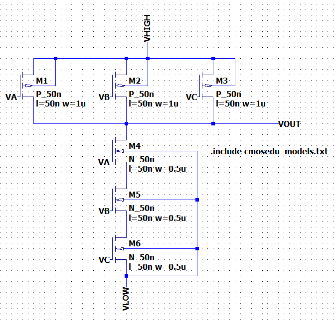
Figure 1. Final schematic of the 3-input NAND gate.
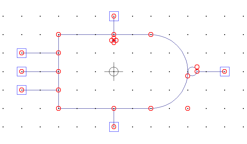
Figure 2. Final symbol of the 3-input NAND gate.
I then used the symbol to simulate the design to confirm it was
functioning properly. The simulation schematic is shown in Figure 3
below. I used pulse functions of varying frequency so that I could
confirm all possible inputs in one simulation. I did confirm this after
checking for all possible cases along the time axis, so 000 to 111 have
been verified this way. The LTSpice simulation waveform is shown in
Figure 4 below. The 3-input NAND gate is always HIGH when at least one
zero is present in the inputs, so the only way to get a LOW output is
if all inputs are ones.
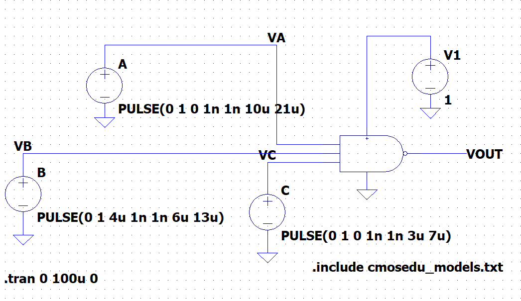
Figure 3. Simulaton schematic for the 3-input NAND gate.
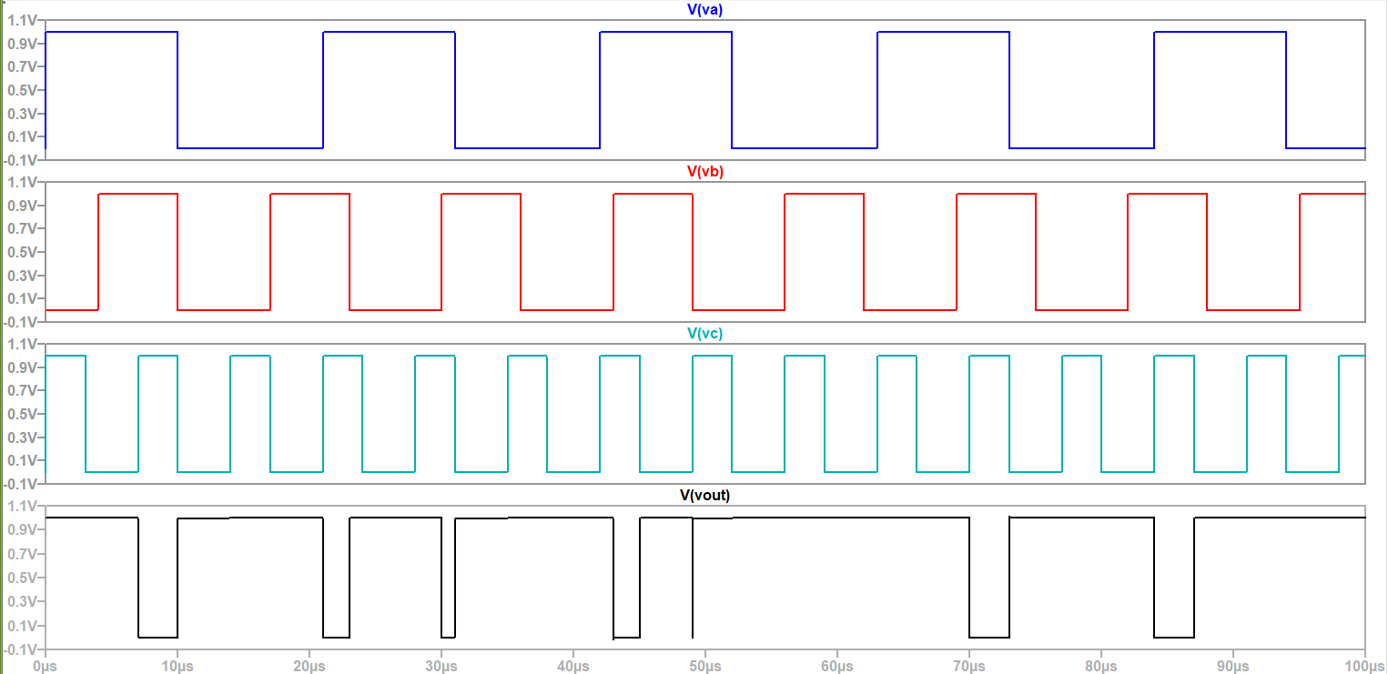
Figure 4. LTSpice simulation waveform results for the 3-input NAND gate simulation.
Task 2: TI DFF.
The next design to be created was the TI DFF or, the Synchronous DFF
with added set and reset functions as it was described in class. This
DFF is based on a design made by Jack Kilby and only requires NAND
gates to be implemented. An image of the schematic for this design was
provided to us and was covered in class so, creating the schematic was
straightforward now that the 3-input NAND gate has been created. The
final schematic for the TI DFF is shown below in Figure 5 in addition
to the schematic's symbol in Figure 6.
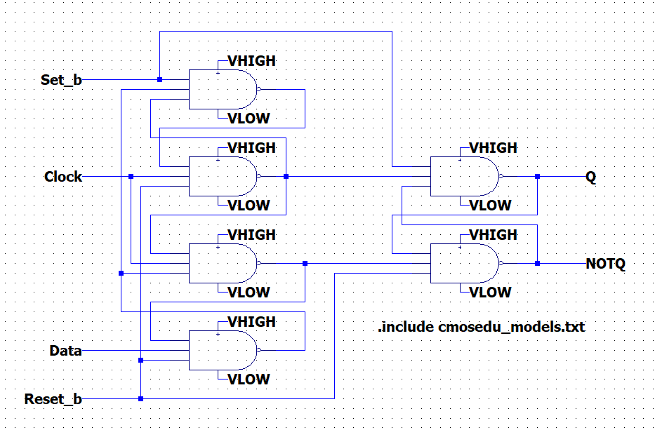
Figure 5. Final schematic of the TI DFF.
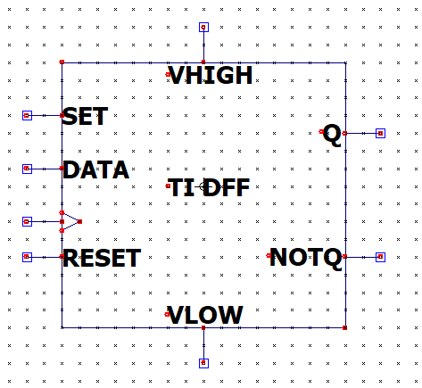
Figure 6. Final symbol for the TI DFF.
Now that the symbol was created it was time to simulate the TI DFF's
functionality. Once again I opted to create PULSE functions for the
inputs that would handle simulating the various functions of the TI
DFF. The simulation schematic used is shown in Figure 7 and the LTSpice
simulation results are shown in Figure 8. The TI DFF performs as
expected when the set and reset inputs are set to HIGH in the four
possible combinations. The Q and Qnot outputs also match what is
expected for each case and the outputs update on the positive rising
edge of the clock signal.
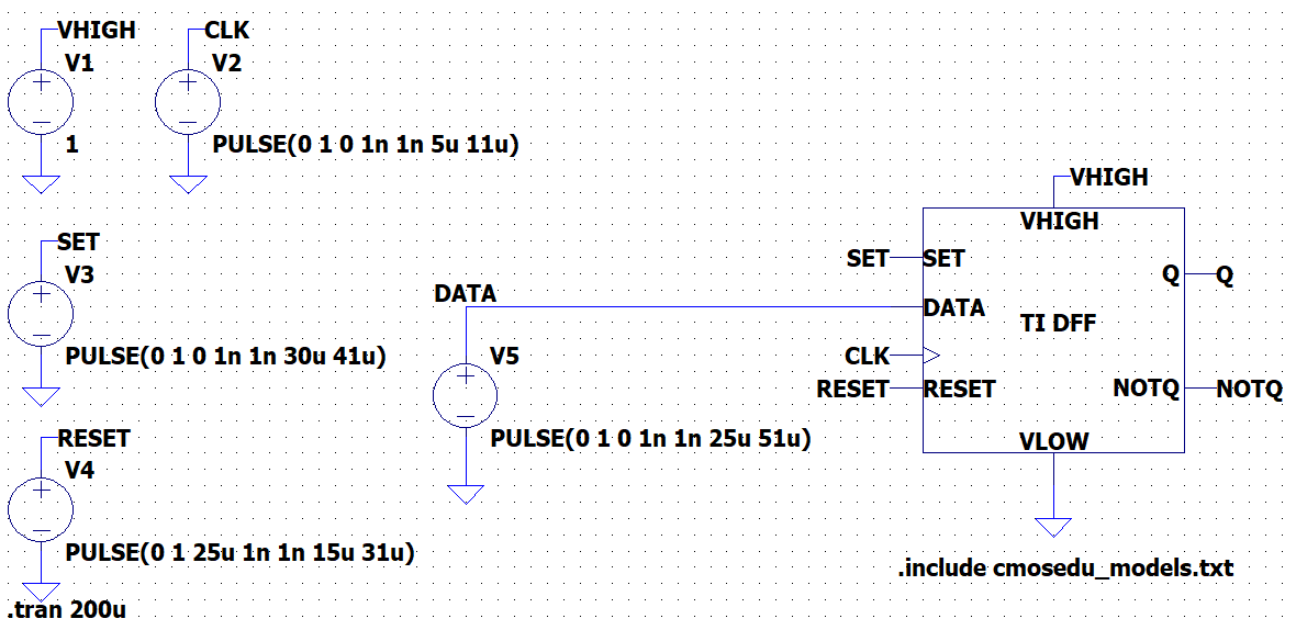
Figure 7. Simulation schematic for the TI DFF.
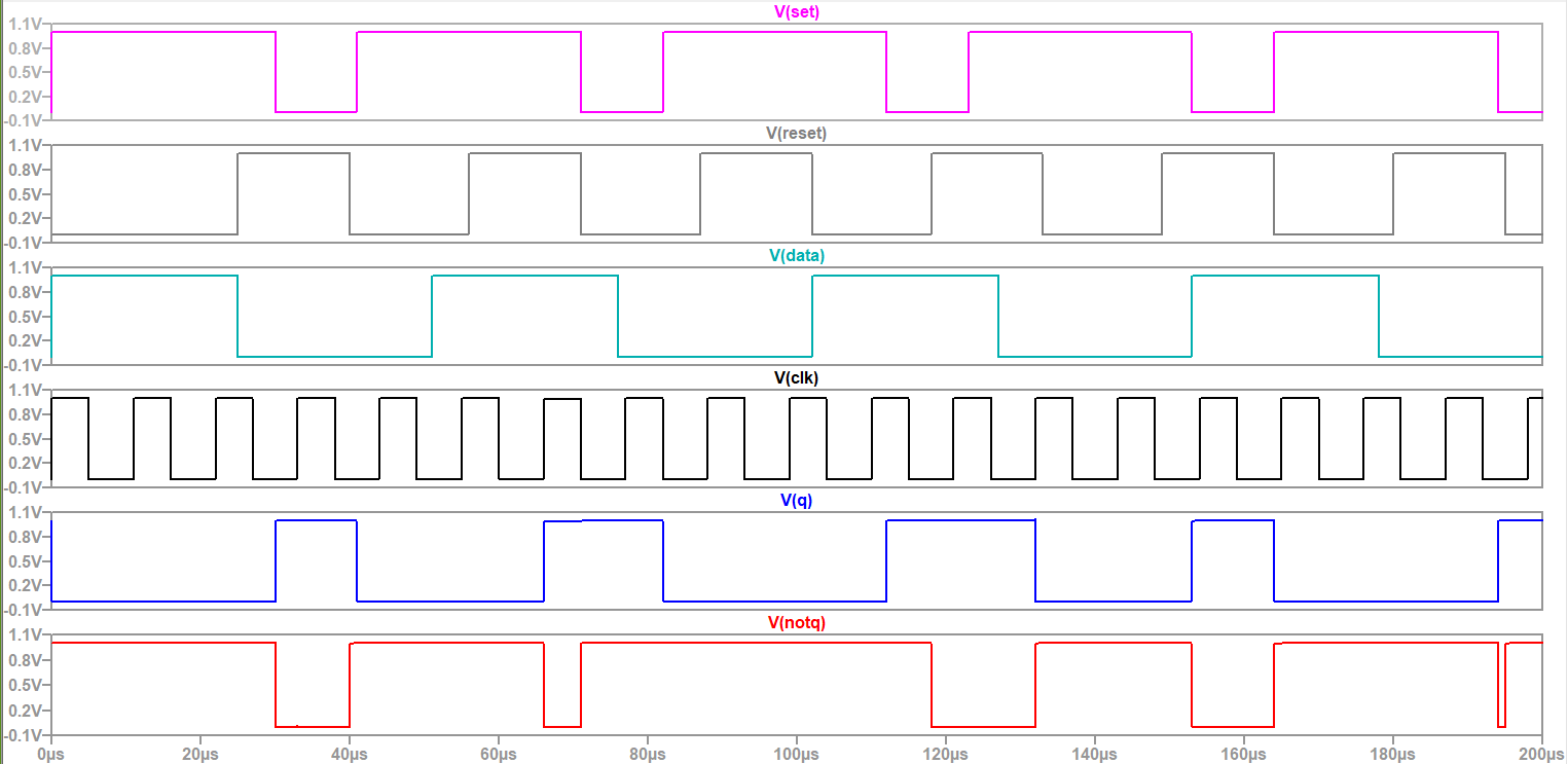
Figure 8. LTSpice simulation waveform results for the TI DFF.
Task 3: 8-bit SAR Block.
The final design to be created was the 8-bit SAR block which makes use
of the TI DFF design. An image of the schematic for a 4-bit SAR block
was provided to us to see the overall structure of a SAR block and it
was up to us to implement the 8-bit version. The 8-bit version of the
SAR block uses 18 TI DFF, there are two TI DFFs for each bit, (8 * 2 =
16) plus two additional ones. Implementing this design was fairly
straightforward since we covered the SAR design previously in this
semester. The comparator input signal plays the role of telling the SAR
if the binary out signal should be increased or decreased. This
comparator would be comparing the DAC signal with the original analog
signal for the purposes of converting an analog signal to be used in
some digital system like recording music to be played back via
speakers. The final schematic of the 8-bit SAR block is shown below in
Figure 9. After completing the schematic the symbol for the SAR was
created as shown in Figure 10.
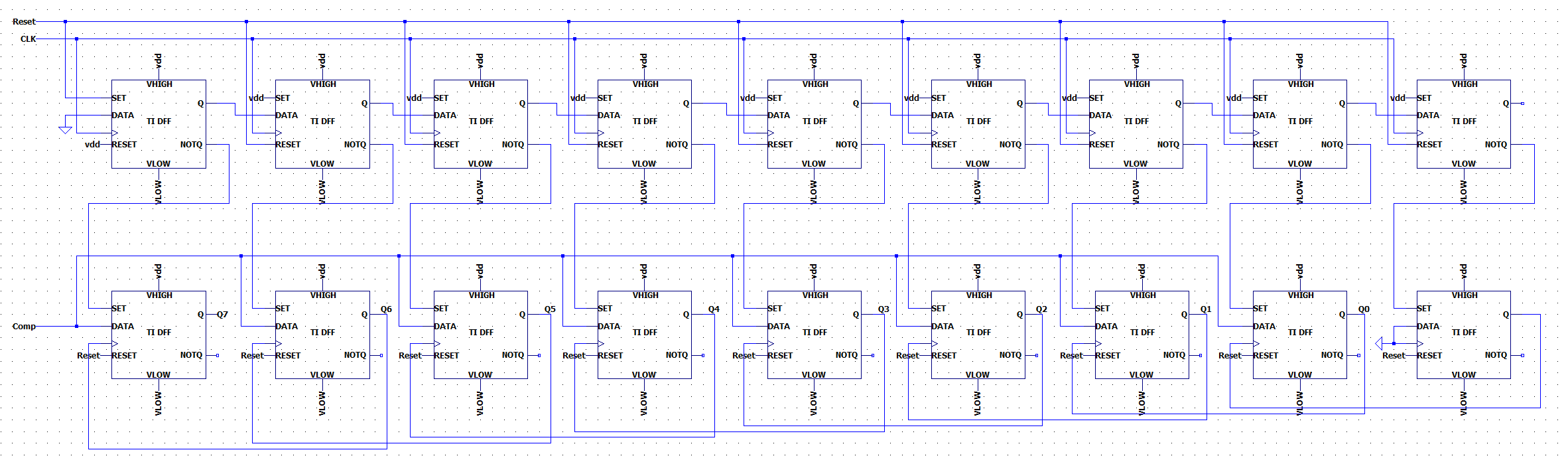
Figure 9. Final schematic of the 8-bit SAR block.
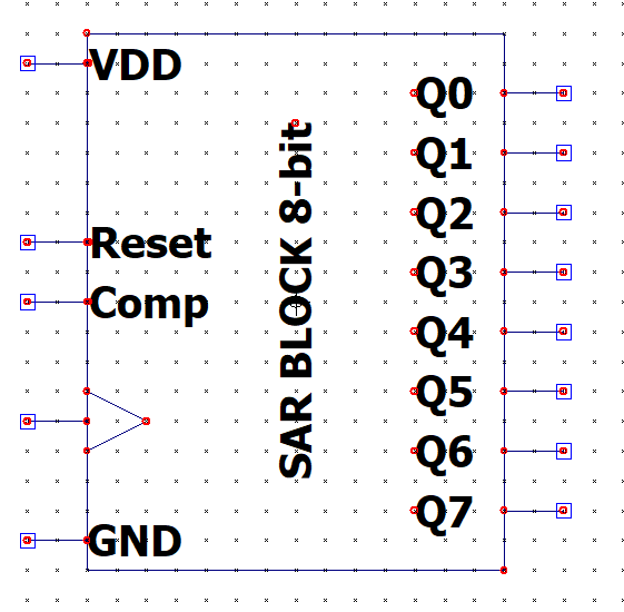
Figure 10. Final symbol of the 8-bit SAR block.
Next a simulation schematic was created for the purposes of verifying
the design's functionality. I decided to use the PULSE function values
provided in the last image of the Final Project Guidelines. The
simulation schematic is shown in Figure 11 while the LTSpice simulation
results are shown in Figure 12. As you move right on the x-axis the
comparitor signal is telling the SAR block whether to keep the current
Q value being set or to change it. The SAR block begins at the 1000
0000 output point, if the signal is too low then the output becomes
1100 0000 and now this value is checked by the comparator to see if it
is too high or too low. At the end of the x-axis the output is 0101
0101 which confirms the SAR block is functioning correctly.
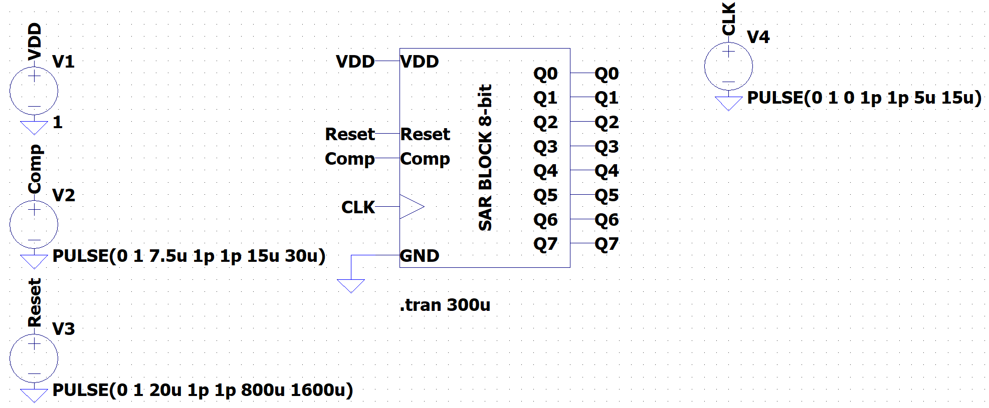
Figure 11. Simulation schematic for the 8-bit SAR block.
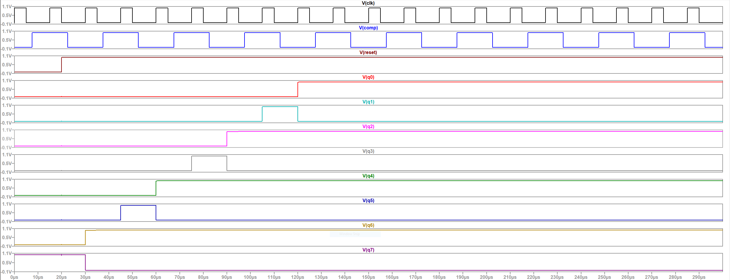
Figure 12. LTSpice simulation waveform results for the 8-bit SAR block.
Discussion
This final project provided great insight into how the SAR ADC block
could be implemented using AOI logic. Since this design is based only
on 3-input NAND gates we could apply our skills gained from using
Electric VLSI to create a layout for the design. It would be pretty
complex since our previous lab had a huge layout whenever we created
the 8-bit ALU. The layout of this SAR block would be similarly big. I
also relearned some LTSpice skills since it has been a while since I
used LTSpice exclusively for circuit simulation. I enjoyed completing
all the designs and creating the symbols. It was also awesome to see
correct simulation results after building up the designs from the
3-input NAND gate to the 8-bit SAR block. I had some issues at the
start due to the PULSE function I used. I originally had the on time
and period time in the range of 5 to 10 ns but the simulation results I
got were not good. They were either zero or one outputs with some minor
fluctuation for the entire simulation. After experimenting I found that
higher intervals of time resulted in the correct simulation results,
which I attribute to some time delay existing in the circuit.