CE351 - Microcontrollers Spring 2020
Power Supply Circuit for MCUs
Name: Sean Eaton
Email:
smeaton@fortlewis.edu
Power Supply Circuit for MCUs
Introduction
We were tasked with creating
a power supply PCB for our first Microcontrollers assignment this
semester with some added design requirements in order to improve
functionality and usability. Previously in this class the power supply
PCB was usable mainly by utilizing female jumper cables to supply power
to a device or breadboard. This semester had the added requirement of
being breadboard compatible similar to the power supply module we have
been utilizing frequently. In addition to plugging into a bread board,
the user should be able to choose any combination of the power supply's
outputs on the breadboard's two power rails. This design uses two
AMS1117 regulators (5V and 3.3V), which can supply those voltages up to
1A, and two LM2596SX regulators, which can supply those voltages up to
3A. A DC barrel jack connector will supply power from the wall socket
to the entire board.
Part 1: 5V and 3.3V 1A Power Supply
Here is the power supply
module that the 1A circuit is based off of. We have used this module
frequently in other classes and it is capable of plugging into a
breadboard directly. A major goal with our power supply design is to be
able to plug it directly into a breadboard and use it similarily to
this power supply module. Jumper headers on either side of the board
allow us to choose between 5V and 3.3V output.
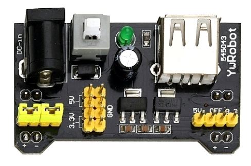
Figure 1. 1 Amp Power Supply Module.
This is the schematic of this power supply module. The important bits
are the AMS1117 regulators and their associated components. We don't
need to incorporate the USB-A port into our design since it is not used
often.
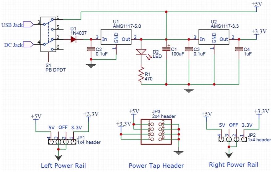
Figure 2. 1 Amp Power Supply Module Schematic.
After taking notes on the available components' footprints (capacitors,
resistors, and diodes), I recreated the schematic in Eagle PCB. The
main modification made was moving the LED and resistor to indicate when
the power supply is receiving power through the DC barrel jack rather
than when 5V is being outputted from the first AMS1117 regulator. I
also created a custom symbol and footprint for the switch availble in
our lab which will function as a ON/OFF switch for the board. After the
first AMS1117 a 5V_1A_OUT net label is created for later use. This also
happens with the second AMS1117 which has a 3.3V_1A_OUT net label.
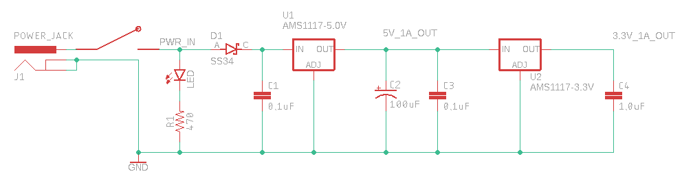
Figure 3. 1A power supply circuit schematic in Eagle PCB.
Now that the 1A power supply circuit schematic was finished I moved onto the 3A power supply circuit.
Part 2: 5V and 3.3V 3A Power Supply
The 3A power supply circuit
is based off the following power supply module, which is able to
provide up to a 3A 5V and 3.3V output. It utilizes a LM2596S voltage
regulator instead of an AMS1117 as well. The circuit schematic was also
generated via Texas Instrument's online app which provides what
inductor and capacitor values should be used based on your inputted
parameters (voltage range, temperature, current output, and voltage
output).
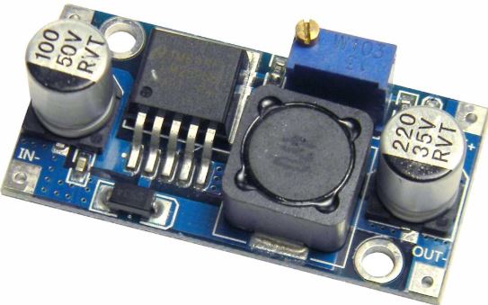
Figure 4. 3A Power supply module.
The follow schematic was implemented in Eagle PCB based off of TI's
online app's schematic. The PWR_IN net label connects this part of the
schematic to the DC barrel jack input which can be seen above in Figure
3. Net labels for the 3A 5V and 3.3V are also created for later use.
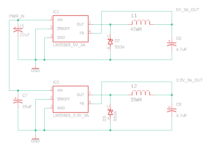
Figure 5. 3A power supply circuit schematic in Eagle PCB.
Now that the main part of the power supply schematic was complete, I
needed to decide how to implement the breadboard compatibility into the
design. I originally wanted to use the 3-pin switches to control the
outputs but I was concerned about accidentally putting two different
voltage sources in parallel. In order to just avoid this issue
completely I decided it was simpler to use jumper headers to control
the output (like with the power supply module in Figure 1). On the
right side of the schematic I set up header pins for the jumper. While
the jumper is not connecting the pins an open circuit prevents any
voltage from appearing at the outpin pins (OUTPUT_L and OUTPUT_R). Once
connected a jumper will short the output choice to the pins that
connect to the breadboard.
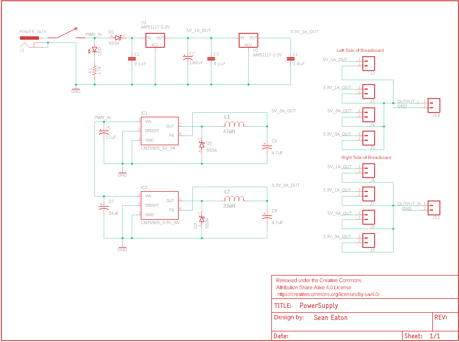
Figure 6. Entire power supply module schematic.
Once the schematic was completed I began designing the board layout.
The first thing I did was measure a breadboard I had available so that
the power supply PCB would have similar dimensions. The width of my
breadboard was about 5.5 cm or 55 mm. I measured the distance between
the header pins on the 1A power supply module, which turned out to be
about 5 cm. Using these measurements I then placed the header pins near
the bottom (with the header pins controlling outputs above them). I
then placed the various other components trying to conserve space and
minimize distances between components that need to be connected
together. After I was happy with the layout I then edited the default
trace width to be 40 mil and autorouted the design as was specified in
the tutorial. I did need to edit some of the traces due to overlap
errors after running a DRC check but for the most part the autorouter
functioned well. After this a copper pour was done on both the top and
bottom layers which were connected to GND. The board layout can be seen
below in Figure 7. Figure 8 also displays a look at what the PCB will
look like after manufacturing.
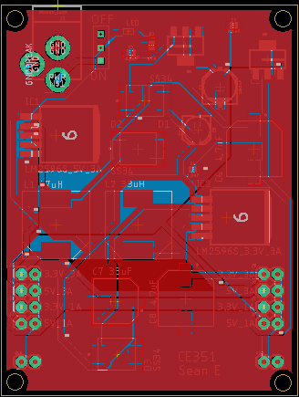
Figure 7. Power supply PCB board layout.
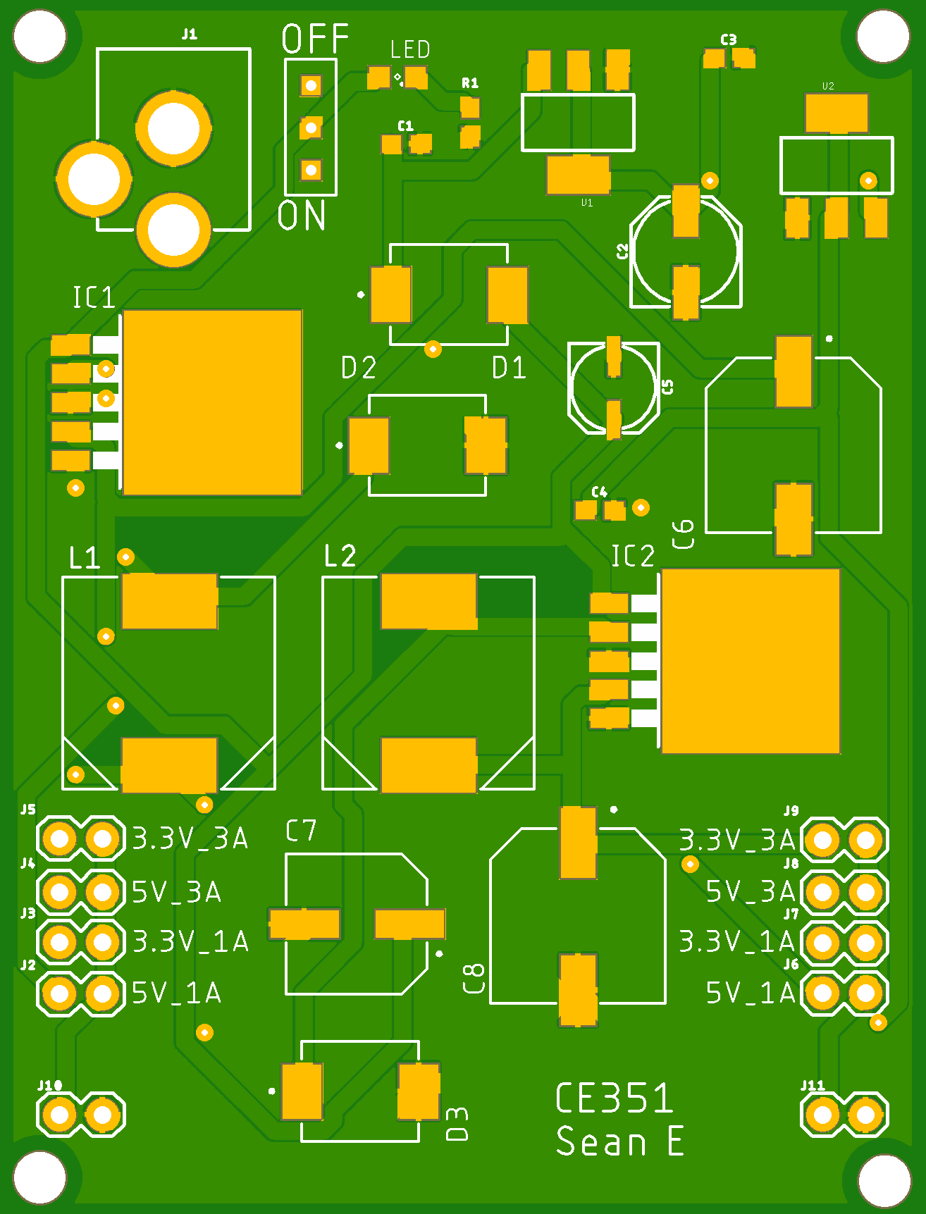
Figure 8. A render of what the power supply PCB will look like once manufactured.
Once the boards have been manufactured the design will be verified
after the necessary soldering is completed. The soldermask was also
verified using Online Gerber Viewer after generating the CAM Outputs
and Gerber Files. The drill file was zipped together with the gerber
files and submitted to PCBway for review as well. The schematic also
passed the necessary ERC check (the only messages were that the header
pins didn't have a value) and the board design passed the necessary DRC
check.
Part 3: PCB Manufacturing and Verification
After
a few weeks the manufactured PCBs were finally received. The power
supply components then needed to be soldered on successfully using
surface mount device components and the design should have its
functionality verified. The completely soldered PCB can be seen below
in.
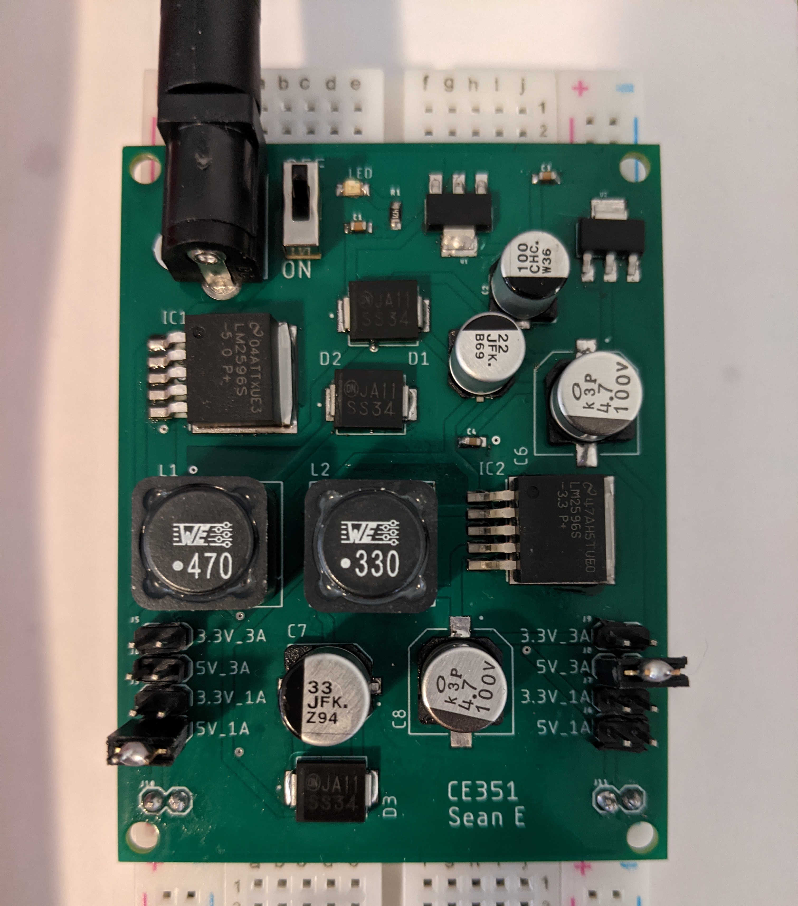
Figure 9. Completely soldered power supply PCB.
After
soldering the components onto the PCB, all of the outputs were tested
to verify the voltage was correct. This was done using a simple circuit
consisting of an LED and resistor so that everything could be seen
visually. All of the outputs worked correctly but only a few images
will be included to show it functioning. Figure 10 shows that the right
side output is able to provide 3.3V using the 3.3V 3A output.
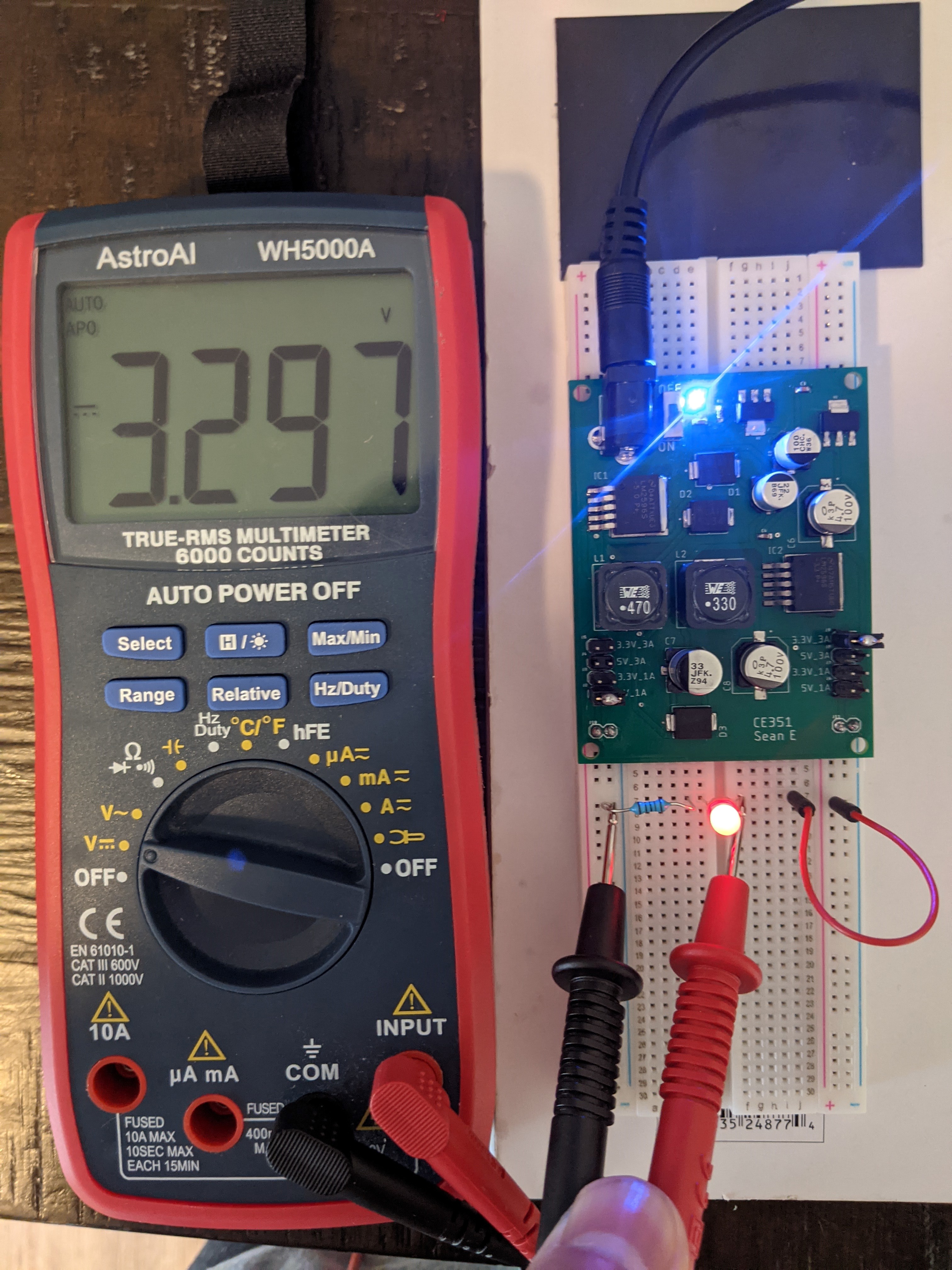
Figure 10. Testing 3.3V 3A voltage output on the right side.
Figure
11 below shows that the current output on the right side is 3.12 mA
(using the 5V 1A output). The current outputs were pretty similar to
one another when using the same voltage output. For example, the 5V
outputs consistently had current measurements near 3.1 mA. The 3.3V
outputs had current measurements near 1.48 mA. This is due to the
circuit not needing to draw very much current from the power supply.
The LED doesn't need to have 1A or 3A current running through it since
it would likely burn out which is why the 1k ohm resistoris neeeded.
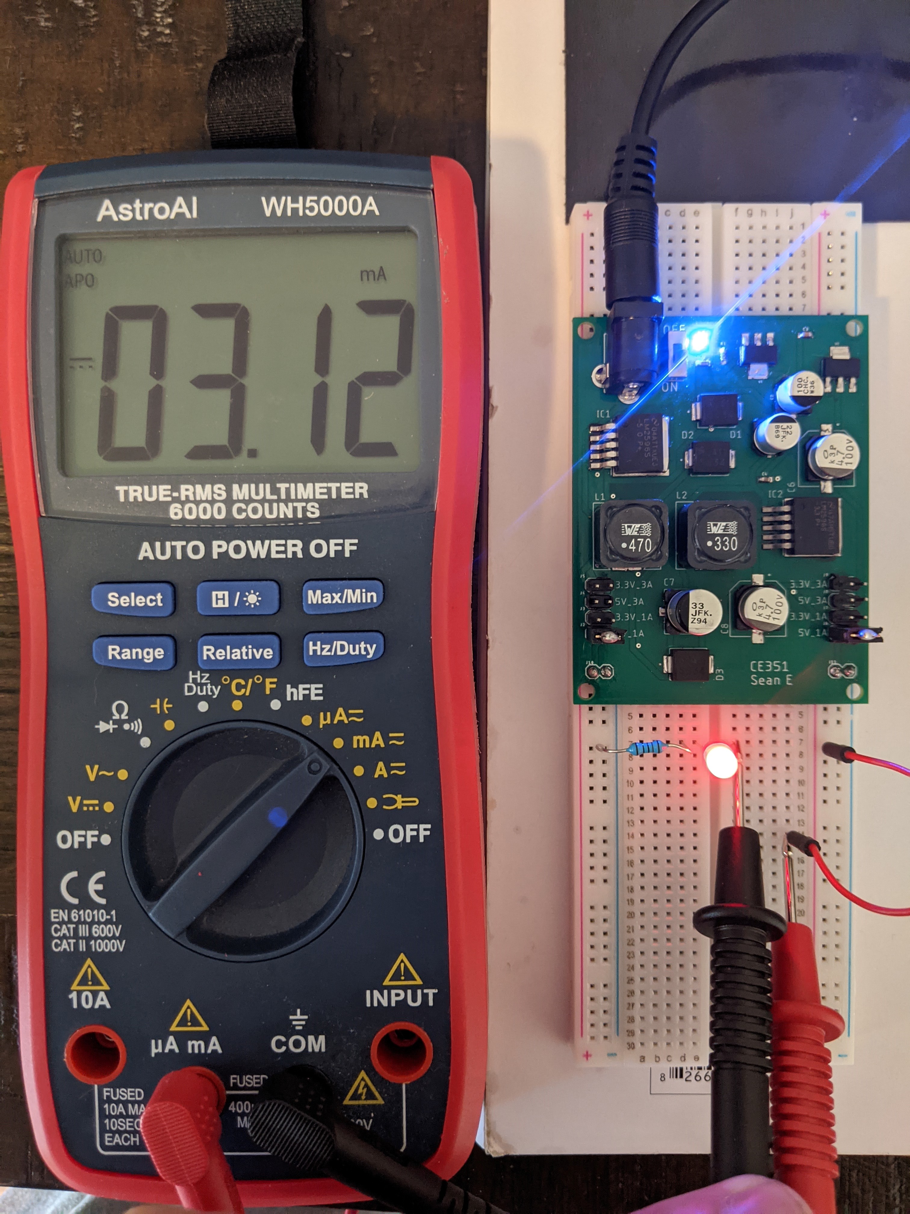
Figure 11. Testing 5V 1A current output on the right side.
Figure 12 below just shows the 5V 3A output providing 5V across the LED and resistor.
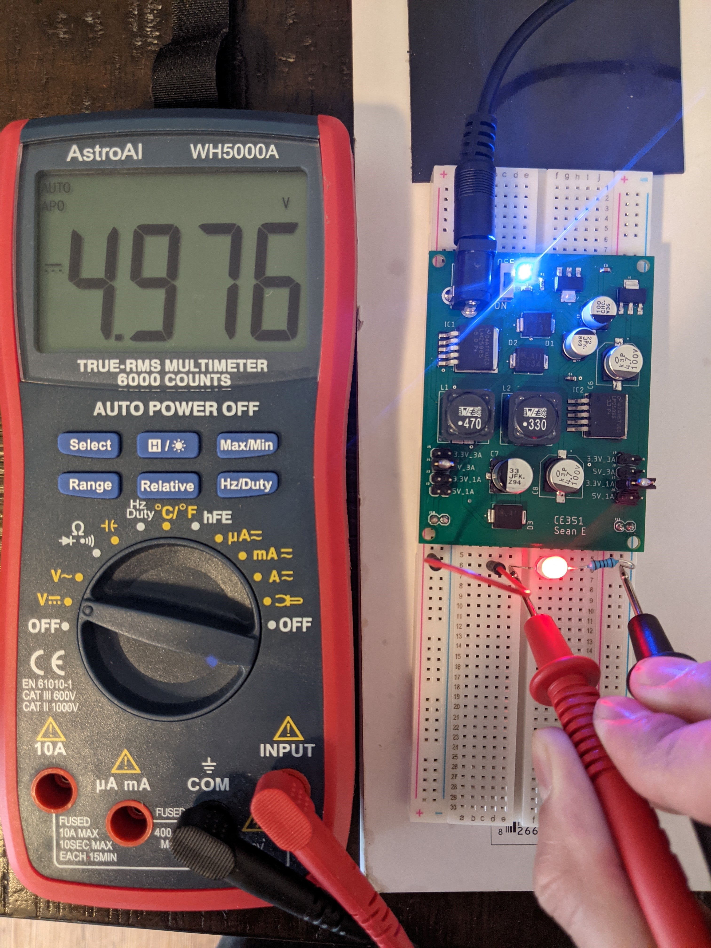
Figure 12. Testing 5V 3A voltage output on the left side.
Conclusion
I enjoyed this assignment, it was interesting to design a PCB that
needed to be breadboard compatible in addition to having flexible
output options. I originally tried to learn Altium Designer but ended
up reverting back to Eagle PCB since the learning process was going a
bit slow for me. I am looking forward to receiving the final product
since this design will come in handy whenever I need a power supply for
any microcontroller. I also enjoyed getting some Altium Designer
exposure since I wasn't aware of it prior to this semester.
After
soldering the PCB I was very happy with its results. It fit into the
power supply rails of the breadboard nearly perfectly. I think one
improvement I can make would be to add aditional header pins to
stabilize the PCB a bit better. The PCB doesn't wiggle around but
additional header pins would ensure there isn't too much stress being
put on the header pins currently included. I also didn't realize that
there wasn't a silkscreen label indicating which header pins are ground
and VCC. I am glad I am able to use this power supply module for a wide
variety of projects as well.