CE 351 2020 Fall
Lab 3: SSD Control
Nic Theobald
nstheobald@fortlewis.edu
SSD Control
Introduction
Arduino can simplify the control of outside systems. With only a
few pins, LEDs can be flashed, transistors can be activated, and signal
can be generated. However, the arduino only has so many pins.
Microcontroller boards that have fewer pins can greatly benefit from
pin reduction techniques such as shift registers and digital decoders.
Materials
Material List
Item
X
Arduino IDE
1
22 OHM R
11
Arduino
1
LED
8
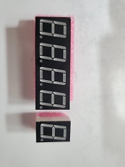
SSD
1
4 dig SSD
1
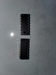
Shift Register
1
Digital Encoder
1
Abbreviated Methods The single SSD was connected to the arduinos
digital pins out. The pins were turned on and off in order to flash the
SSDs. Next the SSD was connected to a Digital Decoder that took in a 4
bit binary number and used its internal logic to switch on an off its
own pin outs. Next, the SSD was connected to a shift register that
required a clock signal, a data pin, and a latch pin. The shift
register output pins were connected to the SSD. The same was used for
the four digit SSD.
Results
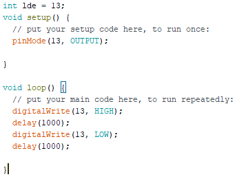
Task: Flashing Pin 13
The first step in this lab was to flash pin 13...
Figure 1: Manually displaying
numbers on SSD.
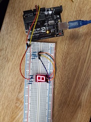
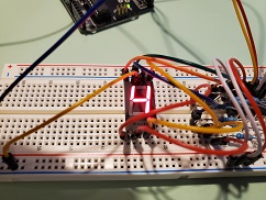
Task 1: Manual Switching
The arduino was directly connected to the SSD through 220 OHM
resistors. Numbers could be displayed by connecting and disconnecting
pins manually.
Figure 2: Manually displaying
numbers on SSD.
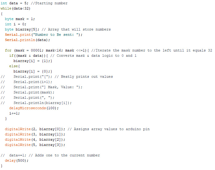
Task 2: Digital Decoder Switching
The Digital Decoder was then added to reduced the number of pins
and to make the number changing process a little more automated. A bit
mask was used to interpret the desired number and set the appropriate
arduino pins to HIGH or LOW.
Figure 3: Bit mask used to
assign High and Low values to Arduino pins.
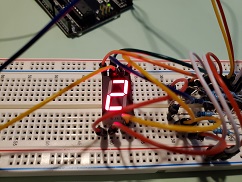
Figure 4: Using Digital decoder
to display numbers on SSD.
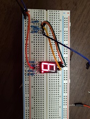
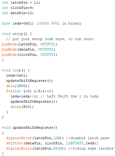
Task 3: Shift Register Switching
The SHift Register was then added to reduced the number of pins
to 1 and to make the number changing process even more automated. A
following code was used to determine the desired sequence and set the
appropriate
arduino pins to HIGH or LOW.
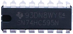
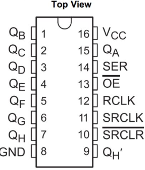
. Figure 5: Shift register IC and Schematic.
Figure 5: Code for controlling shift register
Figure 6: Using Shift Register to Sequence Leds
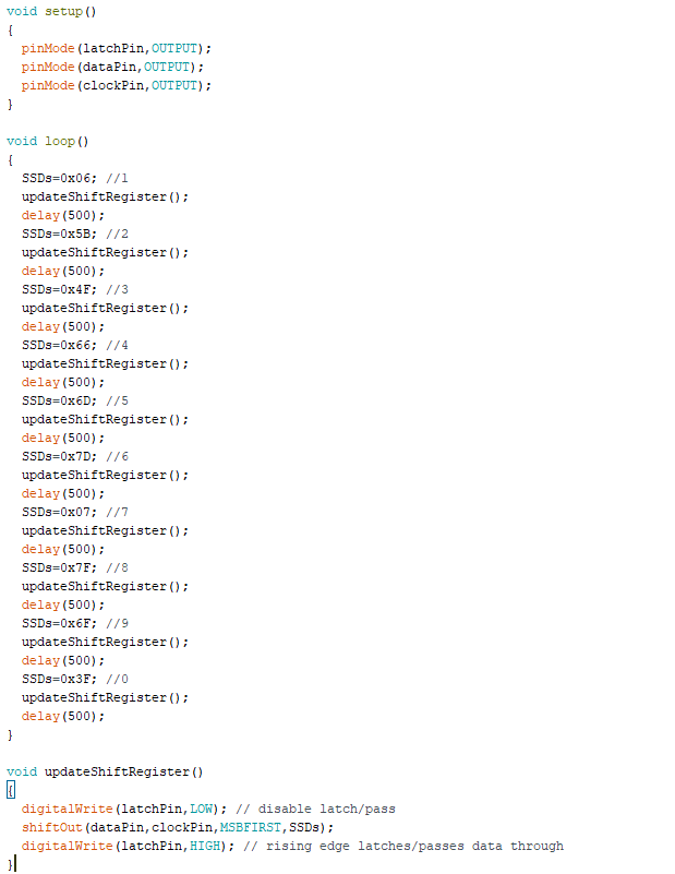
A single digit SSD was then put in the place of the LEDs.
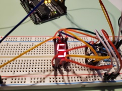
Figure 7: Code for controlling shift register
Figure 8: Using Shift Register to Sequence SSD
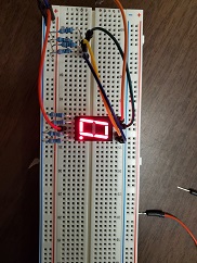
The single digit SSD was then
replace by a four digit SSD and the code was changed to display "2019".
The following code was inserted into a four loop in order to change
the delay over time (for visualization purposes). The code worked by
sending 2 to all of the digits but at the same time only activating
digit one. Then it would send 0 to all of the digit but only activate
digit 2, and so on...
Figure 9: Using Shift Register to flash 2019.
Figure 10: Flashing of "2019" at ever increasing delays.
Figure 11: Flashing of "2019" at constant super fast speed.
Discussion
This lab ultimately demonstrated the power of using shift
registers and digital decoders. Both devices are massively useful in
the optimization of output signals.