ENGR 361 2020 Fall
Lab 1
Power Supply
Nic Theobald
nstheobald@fortlewis.edu
Power Supply
Design
Introduction
This Lab
covers the design of a 3.3V and 5V power supply capable of supplying 1A and 3A.
Eagle PCB and an online Gerber viewer were used to design and verify the power
supply. The PCB was ordered online and the SMD components were soldered on.
Materials
|
Materials |
|
|
Computer |
1 |
|
Eagle
PCB |
1 |
|
Your
Brain |
1 |
|
Some
Patience |
1 |
| SMD Components |
many |
Abbreviated Methods
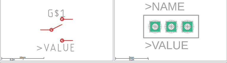
All of
the components for the 3.3V 3A and 5V 3A were made from custom libraries (Figure
1, 2, 3, 4, 5). All of the components were first laid out in the schematic.
All of the parts in the uppermost circuit came with Eagle PCB, but all of the
ones in the lower circuit were made during this lab (Figure 1). New
components were created through the use of custom libraries. All components
were organized on the board before auto routing and the copper pour (Figure
2). Auto routing was performed and the copper pour was completed on top and
bottom layers (Figure 3, 4). The board and schematic were checked
through the use of DRC and ERC checks; the files were also imported into an
online Gerber viewer which helped recognize any mistakes (Figure 5, 6). The SMD components were then soldered to the PCB and the board was tested.
Results
All of
the components for the 3.3V 3A and 5V 3A circuits were made from custom
libraries.
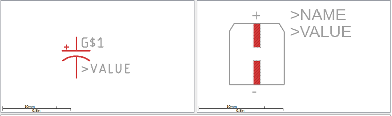
Figure
1: Electrolytic capacitor library.
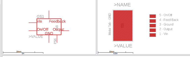
Figure
2: Voltage regulator library.
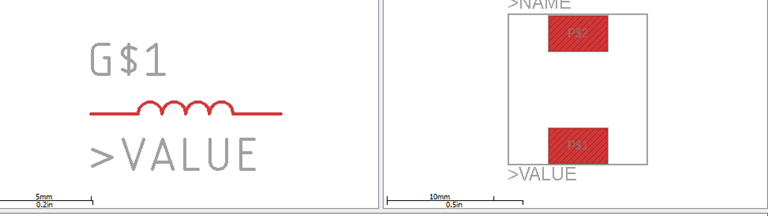
Figure
3: Inductor library.
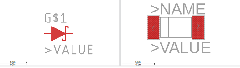
Figure
4: Schottky diode library.
Figure
5: Power switch library.
All of
the components were first laid out in the schematic
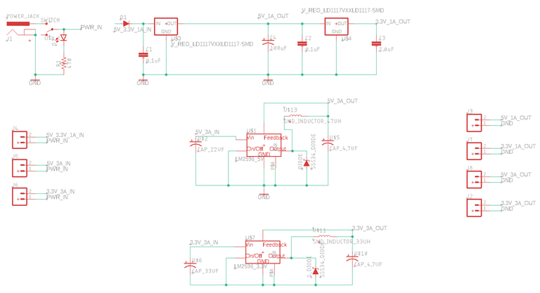
Figure
1: Schematic for power Supply
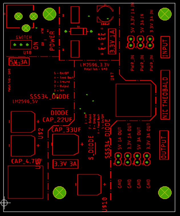
All components
were organized on the board before auto routing and copper pour.
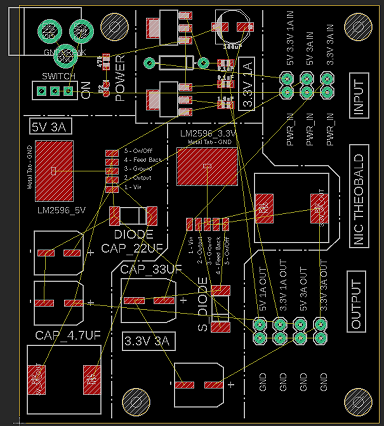
Figure
2: Board before auto routing and copper pour.
Auto
routing was performed and the copper pour was completed on top and bottom
layers.
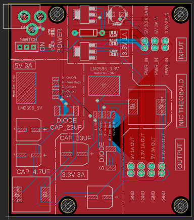
Figure
3: Top layer copper pour.
Figure
4: Bottom layer copper pour.
ERC and
DRC checks were performed before export.
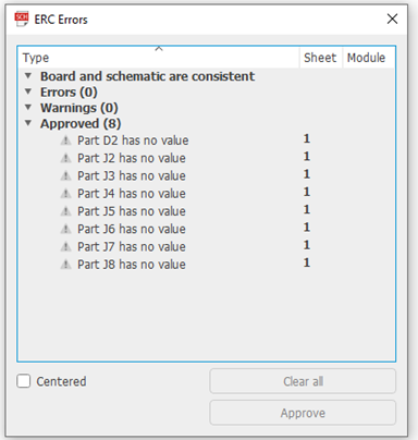

The 8 approved errors were from
unvalued headers…

The
Gerber files were imported into a viewer and drill and silk screen were
confirmed.
Figure
5: Drill and silkscreen.
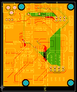
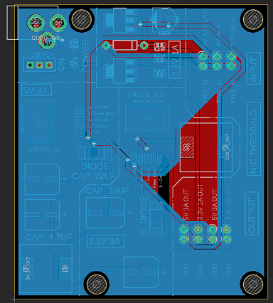
Figure 6: Overview of important details.

Figure 7: The PCB before soldering.
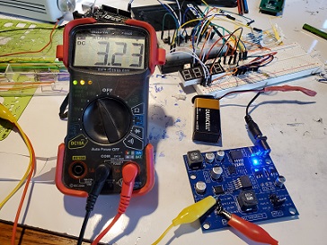
Figure 8: Testing 3.3V 3A.
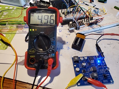
Figure 9: Testing 5V 3A.
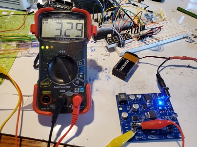
Figure 10: Testing 3.3V 1A.
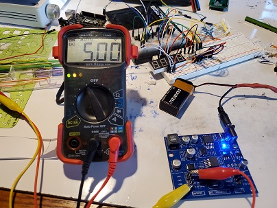
Figure 11: Testing 5V 1A.
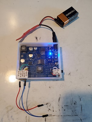
Figure 12: The PCB inside a 3D printed case with a 3 position switch.
Discussion:
Eagle
PCB was used in the design of a
power supply circuit. The circuit was designed to output 3.3V and 5V
with 1A or
3A. The PCB was ordered online and the SMD components were solder on.
Initially, the board was tested but didn't operate correctly. It was
found that the 5V 3A circuit was not grounded. A small amount of solder
mask was scrapped off, exposing the grounded copper layer. The ground
tab of the voltage regulator was then soldered to the exposed copper
and the power supply worked as intended.