CE 338 2021 Spring Final Project: Design of SAR Block
Nic Theobald
nstheobald@fortlewis.edu
Simple 8-bit SAR block
Introduction
This
lab covers the simulation of the Succesive Approximation Register (SAR)
block for a SAR ADC. This block successivly shifts the results of a
comparator to the SAR's output. This allows you to approximate an
analog voltage within 2^n divisions.
Methods and Materials
Item
Quantity
LTspice
Electric VLSI
Ideal ADC/DAC Library
1
1
1
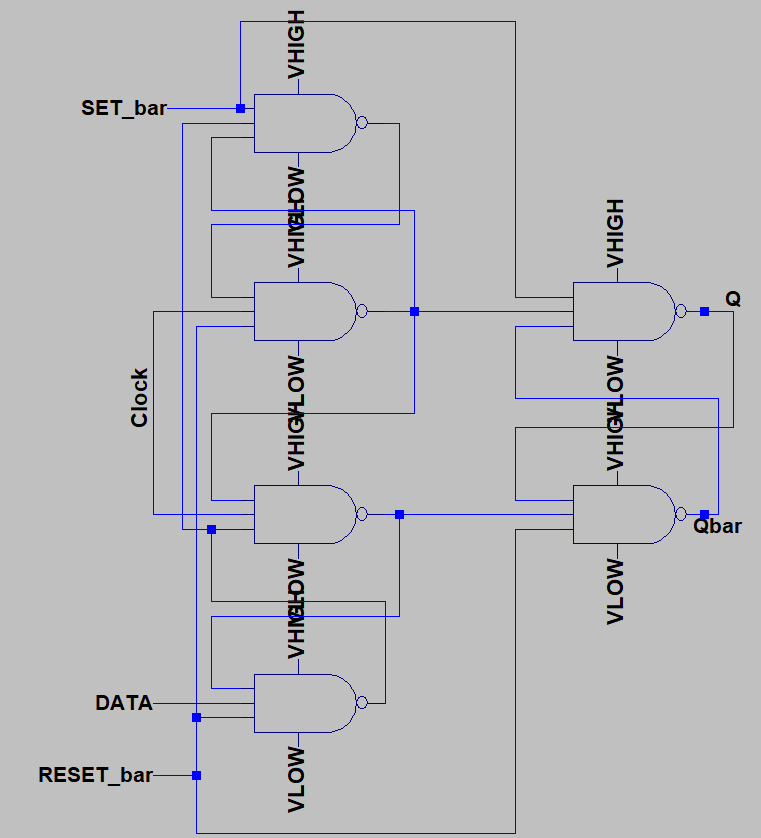
The SAR block was built out of D flip flops which were built
from 3 input Nand Gates. 50 nm technology was used for this lab. A VCC
of 1v was used.
Results
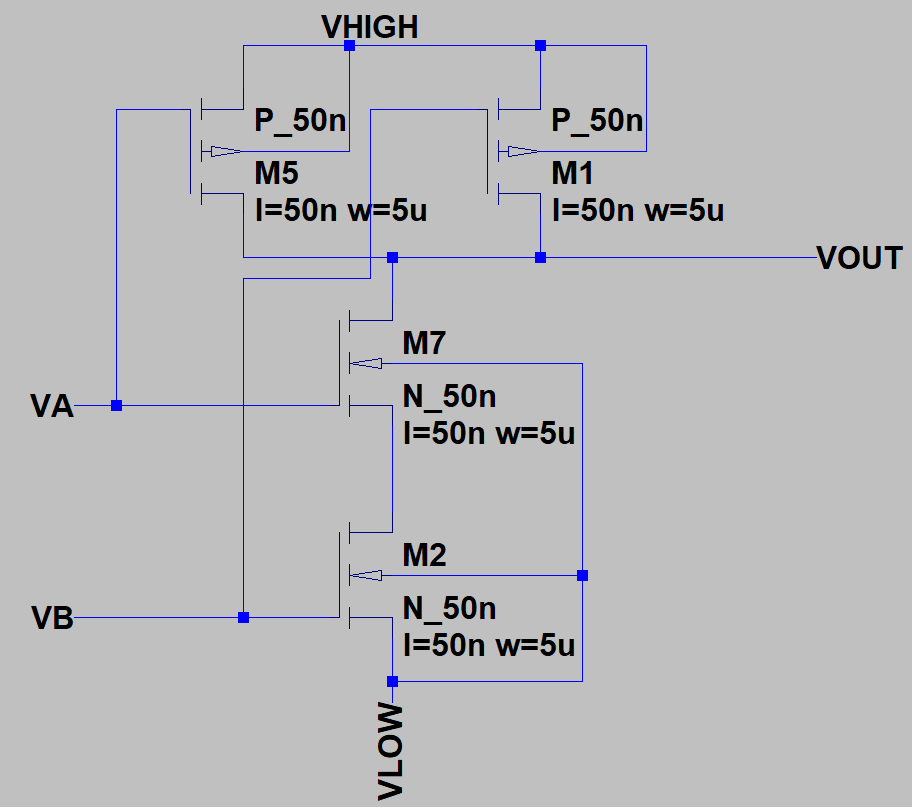
Task 1: Create 3 input Nand The 2 input nand was first
created using 50nm technology. The 2 input nand was turned into a
symbol, which was used to create the 3 input nand.
Figure
1: Creation of 3 input nand.
The 3 input nand was then simulated.
Figure 2: Simulation of 3 input nand.
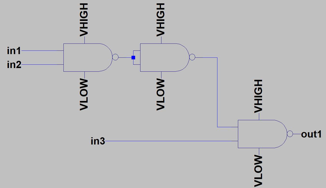
Task 2: Create DFF using 3 input nand
The D flip flop was created from 3 input nand.
Figure 3: DFF from 3 input nand.
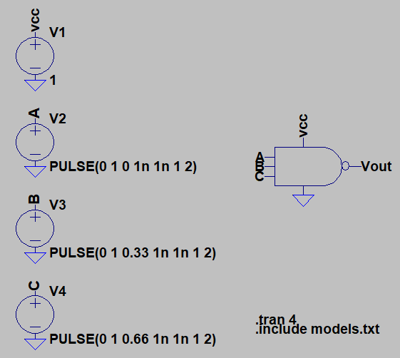
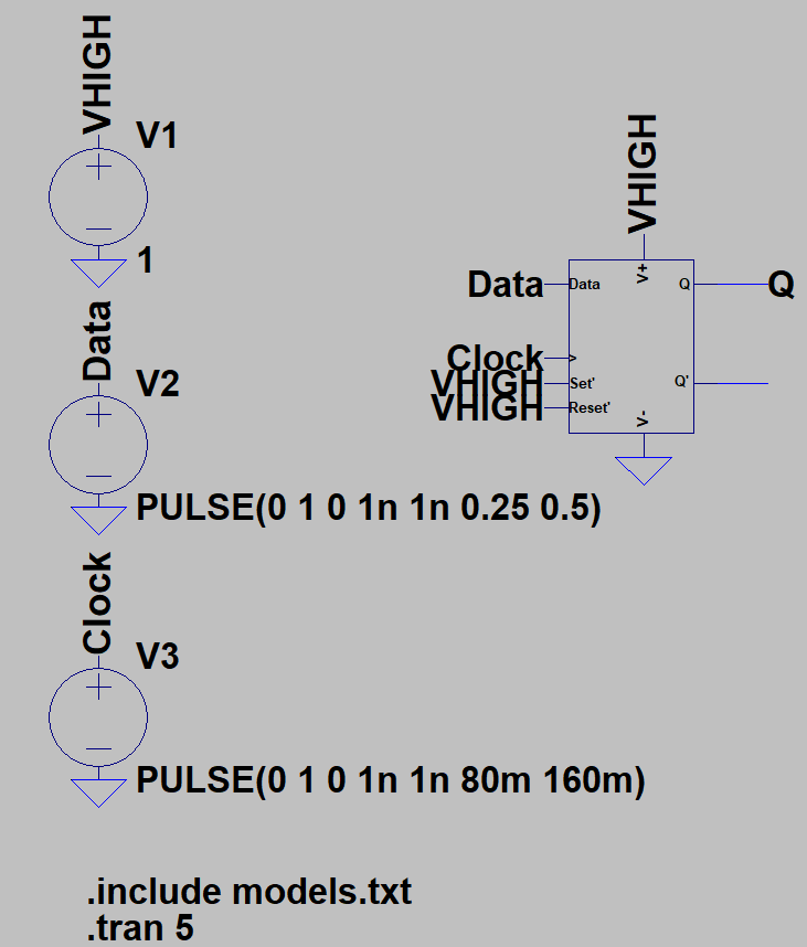
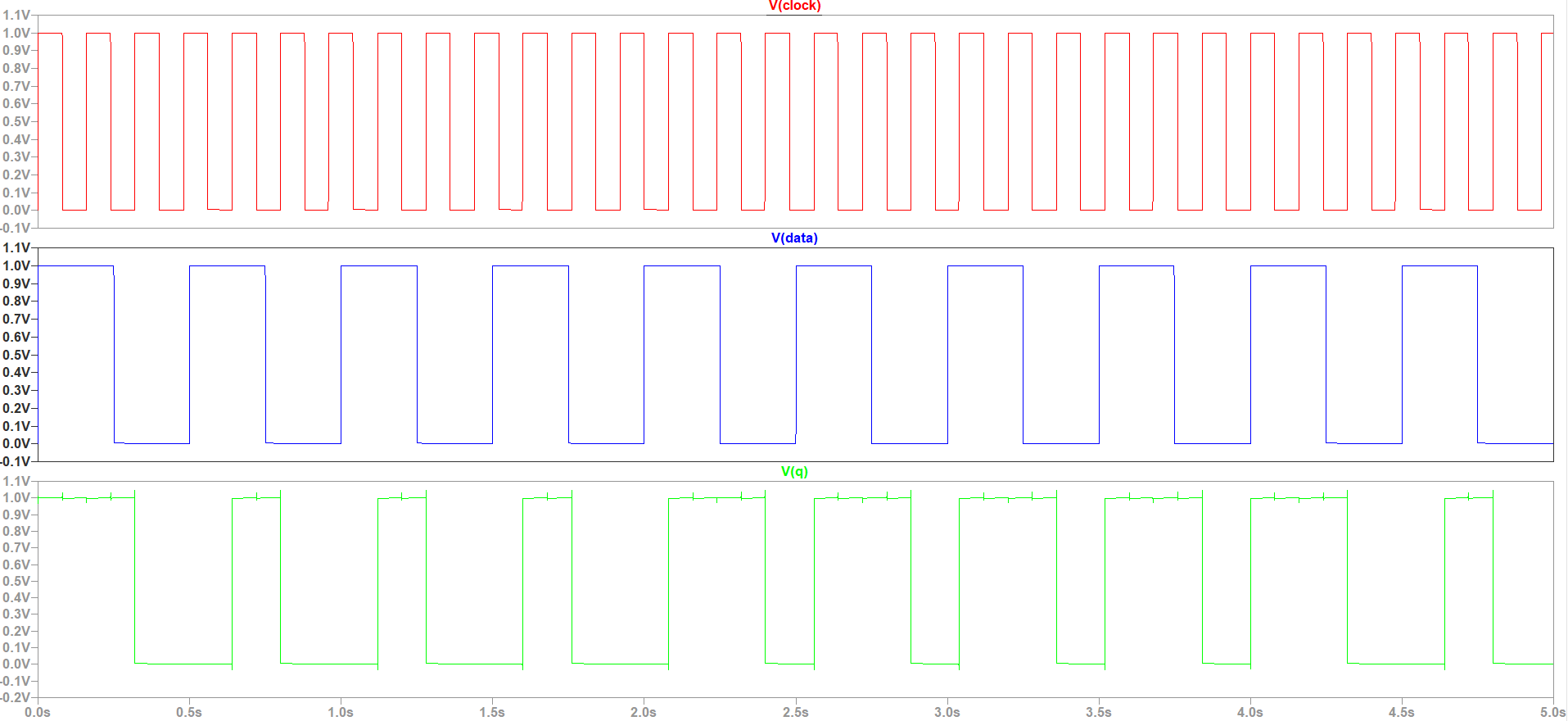
The DFF was packaged into a symbol and was simulated.
Figure 4: Simulation of DFF.
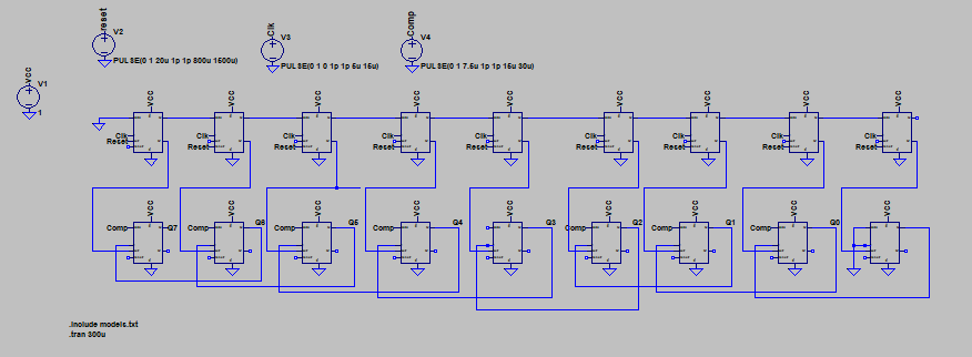
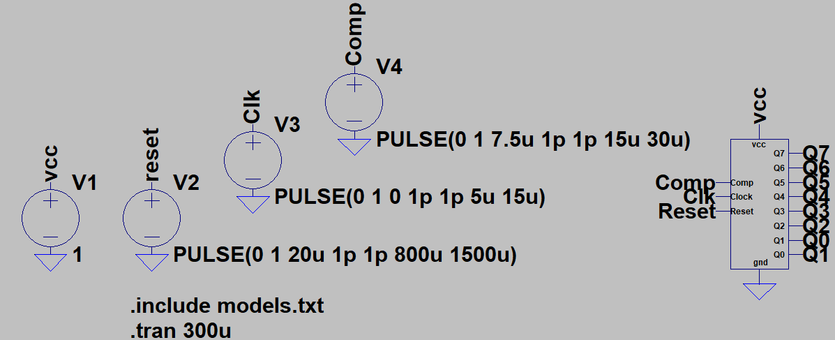
Task 3: Create SAR block using DFF
The SAR block was created using the DFF.
Figure 5: Sar block from DFF.
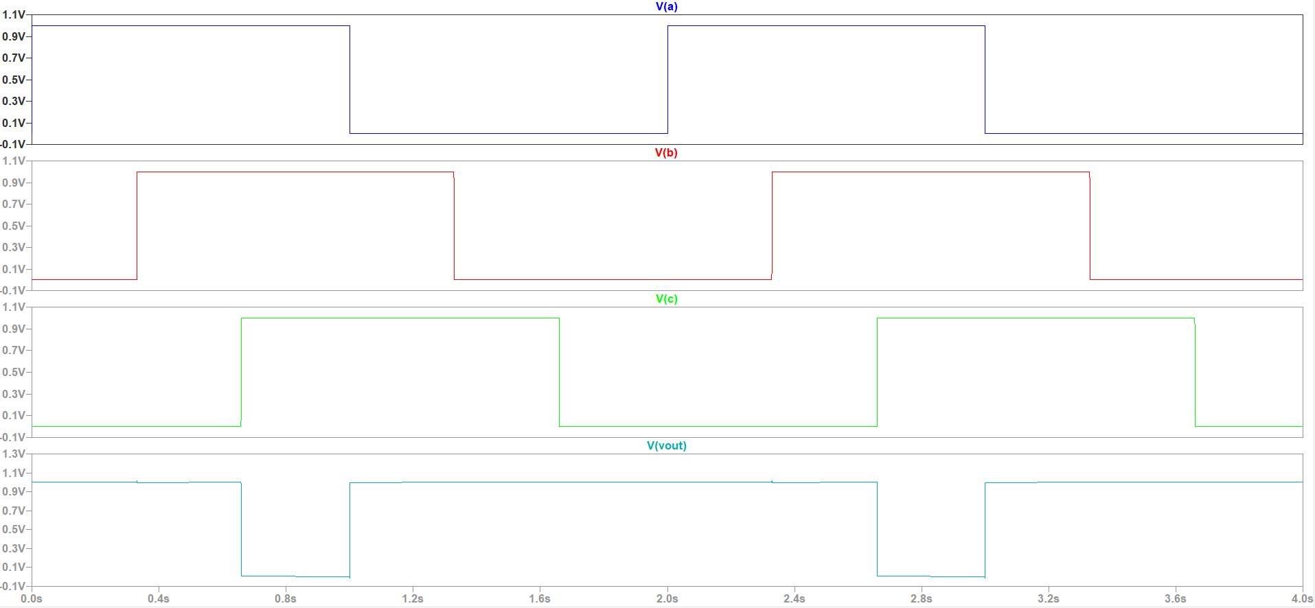
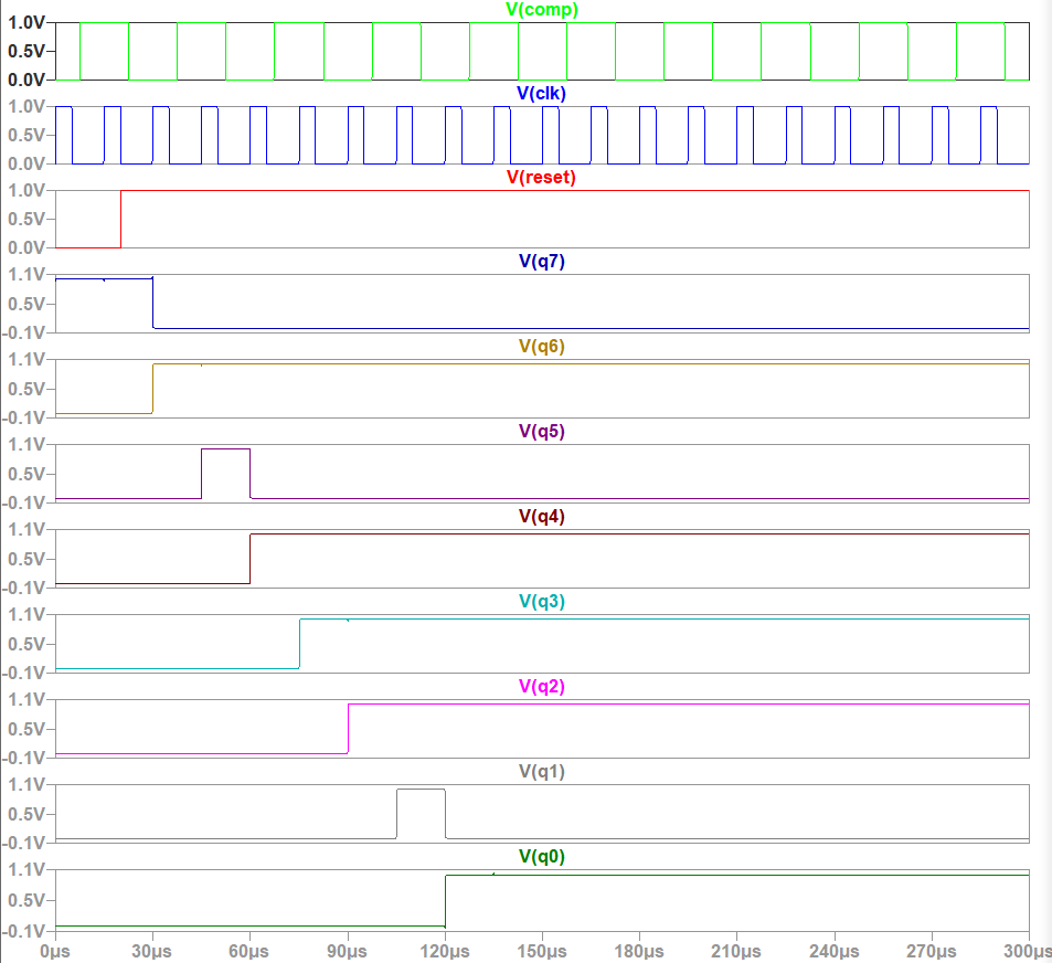
The SAR block was packaged into a symbol and simulated.
Figure 6: Simulation of SAR block.
Discussion:
This lab detailed the design and simulation of an 8 bit SAR block.