CE 338 2021 Spring
Lab 7: Busses
Nic Theobald
nstheobald@fortlewis.edu
Buses in Electric VLSI
Introduction
This
lab covers the design and simulation a ring oscillator and multi-bit gates in electric VLSI.
Methods and Materials
|
|
Item
|
Quantity
|
|
|
LTspice
Electric VLSI
Ideal ADC/DAC Library
|
1
1
1
|
|
|
Schematics using the normal and bus method were created for
the ring oscillator (Figure 1). They were then simulated (Figure 2).
The layout for the bus method was then created and error checking tool
were run (Figure 3, 4). The same process was used for the other logic gates.
Results
Task 1: Build and Simulate a Ring Oscillator
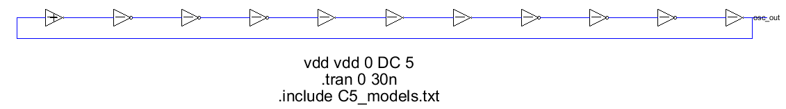
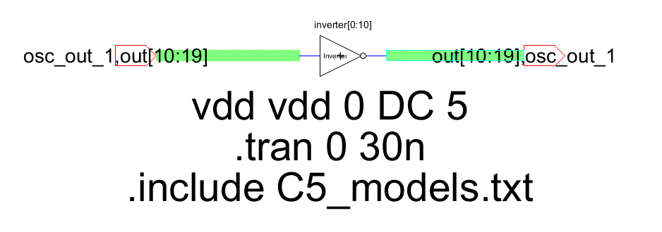
The schematic for both ring oscillators were created. The second schematic shows the use of busses.
Figure
1: Schematic view of the ring oscillator.
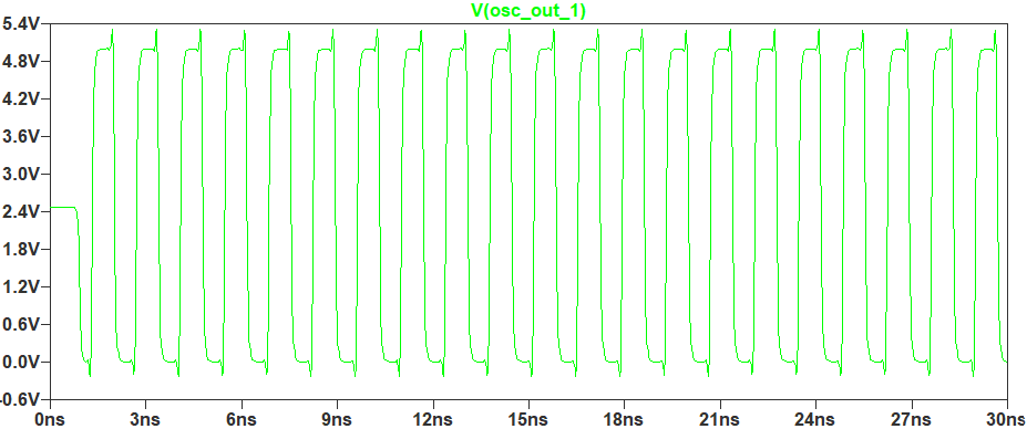
Both methods were simulated in LTspice.
Figure
2:Simulation of ring oscillator.
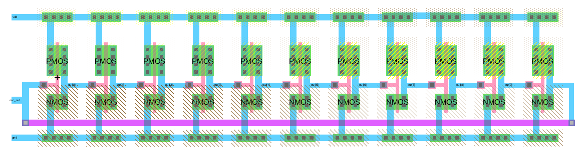
The layout of the ring oscillator was then created.
Figure 3: Layout view of the ring oscillator.
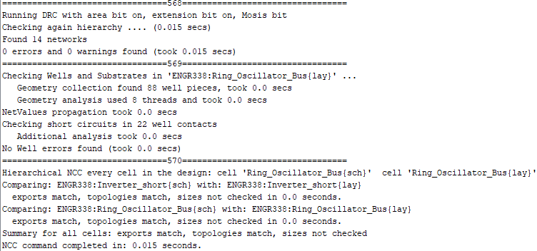
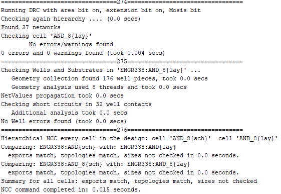
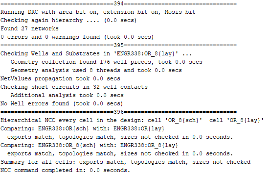
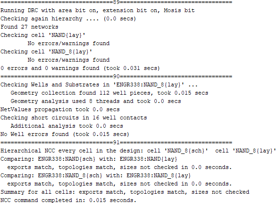
ERC, DRC, and NCC were also checked.
Figure 4: Checking for errors.
Task 2: Design an 8-bit AND Gate
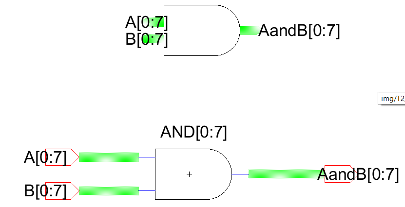
The schematic of the 8 bit and was first created and simulated
Figure 5: Schematic view of the 8 bit and.
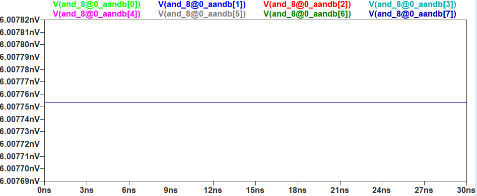
The schematic was then simulated in LTspice.
Figure 6:Simulation on 8 bit and.
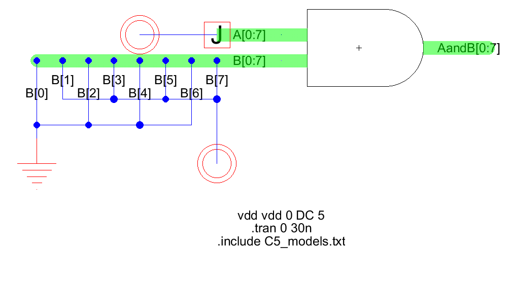
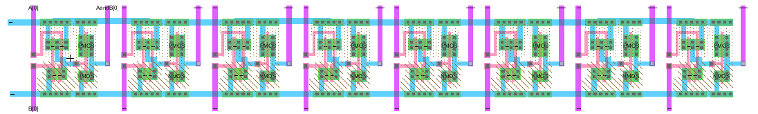
The layout of the 8 bit and was then created.
Figure 7: Layout view of the 8 bit and.
ERC, DRC, and NCC were also checked.
Figure 8: Checking for errors.
Task 3: Design 8-bit OR Gate
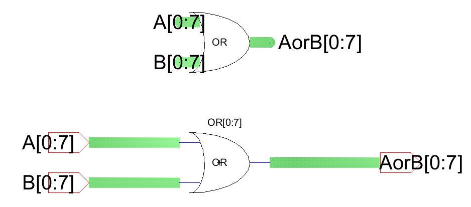
The schematic of the 8 bit or gate was first created and simulated
Figure 5: Schematic view of the 8 bit or gate.
The schematic was then simulated in LTspice.
Figure
2:Simulation on 8 bit or gate.
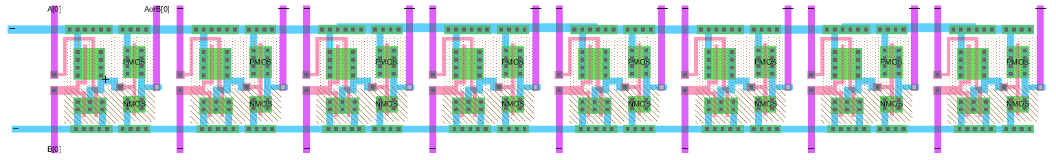
The layout of the 8 bit or gate was then created.
Figure 3: Layout view of the 8 bit or gate.
ERC, DRC, and NCC were also checked.
Figure 4: Checking for errors.
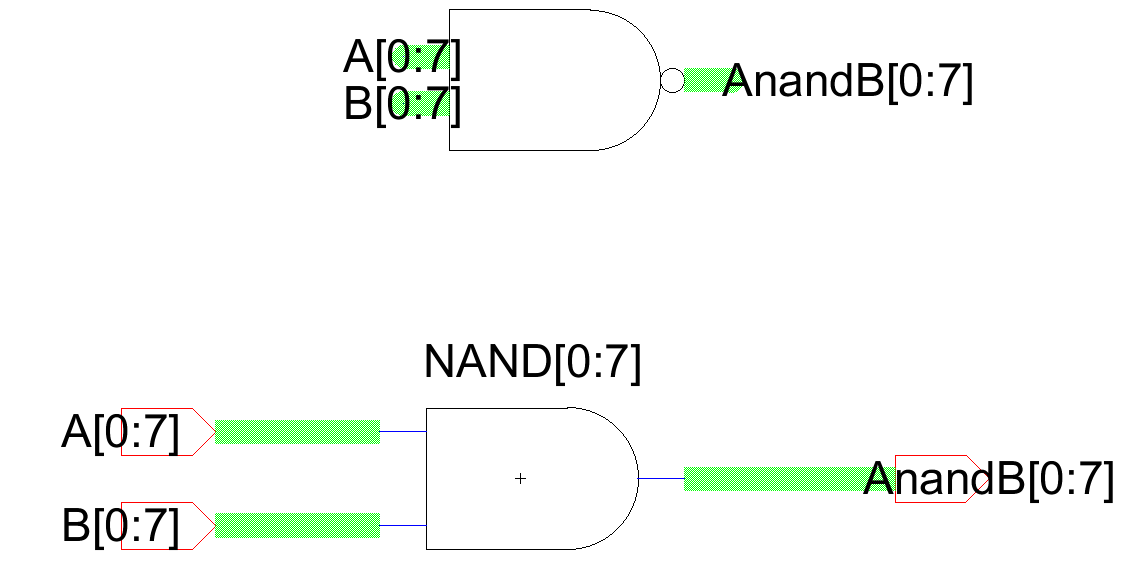
Task 4: Design 8-bit NAND Gate
The schematic of the 8 bit nand gate was first created and simulated
Figure 5: Schematic view of the 8 bit nand gate.
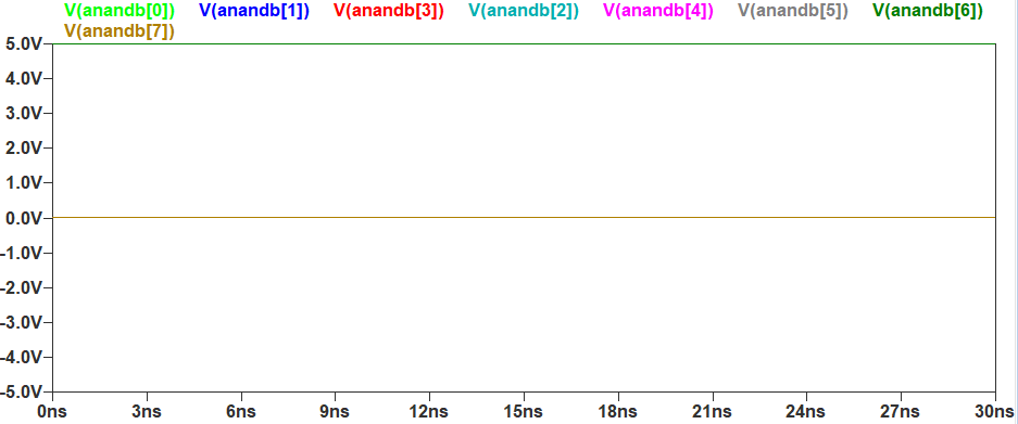
The schematic was then simulated in LTspice.
Figure
2:Simulation on 8 bit nand gate.
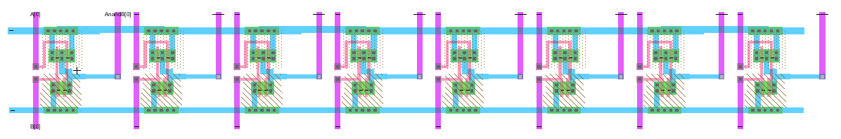
The layout of the 8 bit nand gate was then created.
Figure 3: Layout view of the 8 bit nand gate.
ERC, DRC, and NCC were also checked.
Figure 4: Checking for errors.
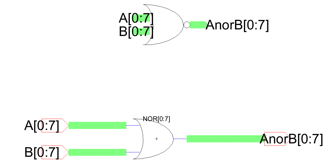
Task 5: Design 8-bit NOR Gate
The schematic of the 8 bit NOR gate was first created and simulated
Figure 5: Schematic view of the 8 bit NOR gate.
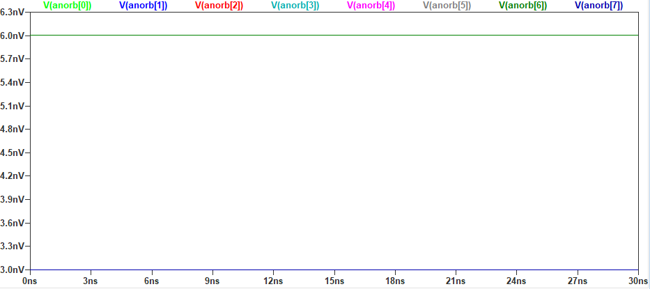
The schematic was then simulated in LTspice.
Figure
2:Simulation on 8 bit NOR gate.
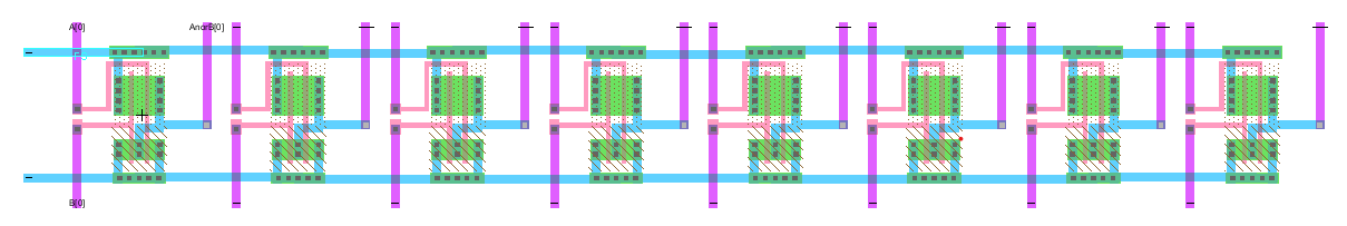
The layout of the 8 bit NOR gate was then created.
Figure 3: Layout view of the 8 bit NOR gate.
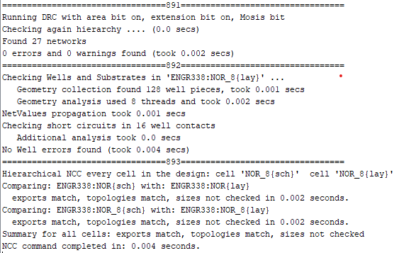
ERC, DRC, and NCC were also checked.
Figure 4: Checking for errors.
Discussion:
This lab detailed the design and simulation of 8 bit logic gates using busses.