CE 338 2021 Spring
Lab 6: NAND, NOR, XOR, and Full Adder
Nic Theobald
nstheobald@fortlewis.edu
NAND, NOR, XOR, and Full Adder
Introduction
This
lab covers the design and simulation of several transistor level logic
gates. Nand, nor, xor, and a full adder were implemented using NMOS and
PMOS transistors. Simulations were performed to ensure that the gates
and adder were performing as expected.
Methods and Materials
|
|
Item
|
Quantity
|
|
|
LTspice
Electric VLSI
Ideal ADC/DAC Library
|
1
1
1
|
|
|
The schematic and icon for each gate was first created. The
Layout of each gate was then created and checked for consistency with
the schematic. Simulations for each gate were also performed.
Results
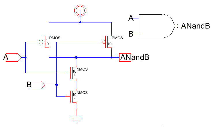
Task 1: Create Schematic and Layout of NAND Gate
The schematic of the nand gate was first created and simulated
Figure
1: Schematic view of the nand gate.
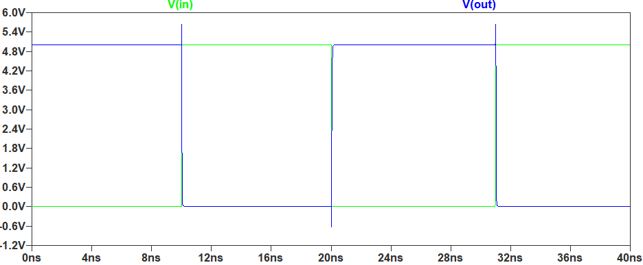
The schematic was then simulated in LTspice.
Figure
2:Simulation on nand gate.
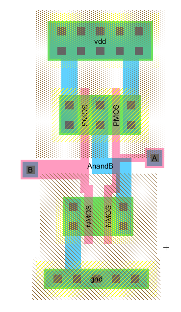
The layout of the nand gate was then created.
Figure 3: Layout view of the nand gate.
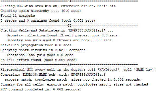
ERC, DRC, and NCC were also checked.
Figure 4: Checking for errors.
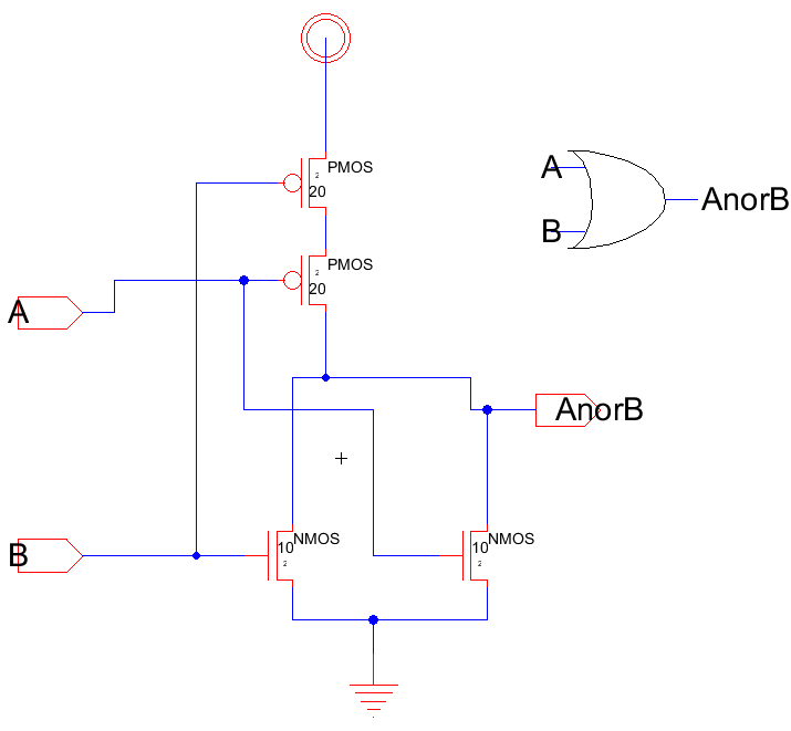
Task 2: Create Schematic and Layout of NOR Gate
The schematic of the nor gate was first created and simulated
Figure 5: Schematic view of the nor gate.
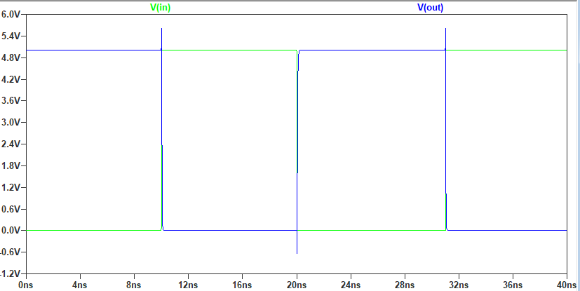
The schematic was then simulated in LTspice.
Figure
2:Simulation on nor gate.
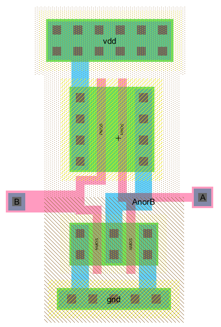
The layout of the nor gate was then created.
Figure 3: Layout view of the nor gate.
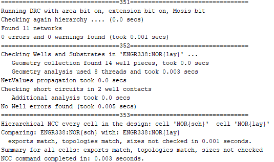
ERC, DRC, and NCC were also checked.
Figure 4: Checking for errors.
Task 3: Create Schematic and Layout of XOR Gate
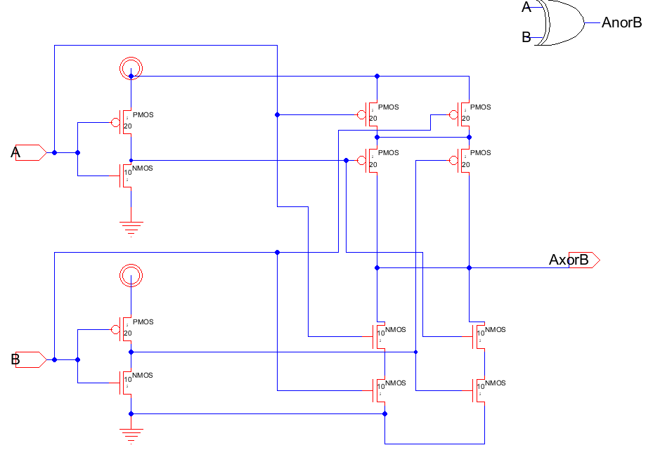
The schematic of the xor gate was first created and simulated
Figure 5: Schematic view of the xor gate.
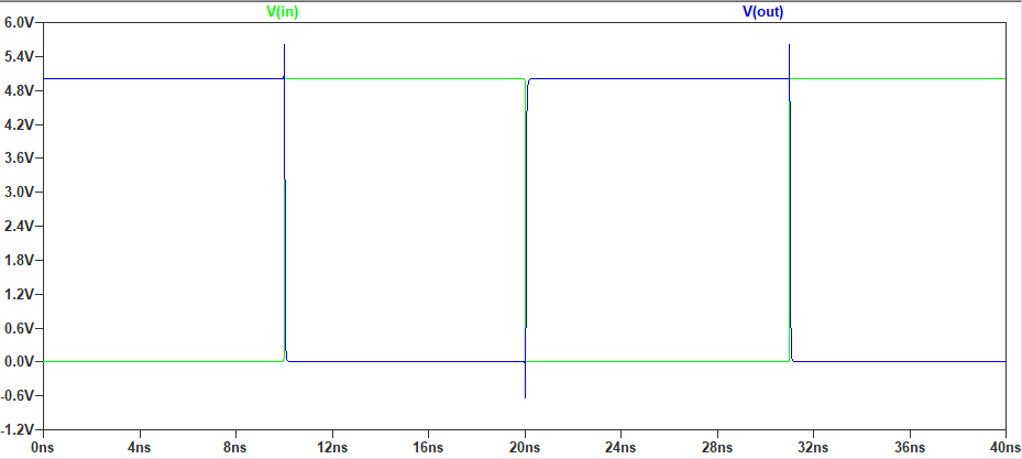
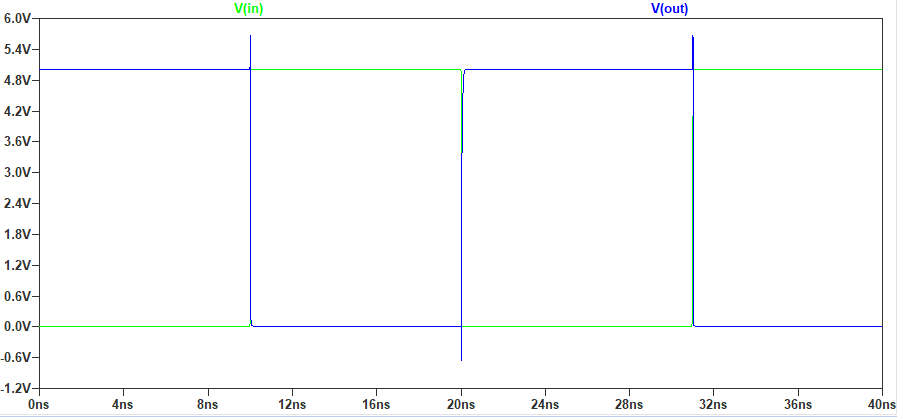
The schematic was then simulated in LTspice.
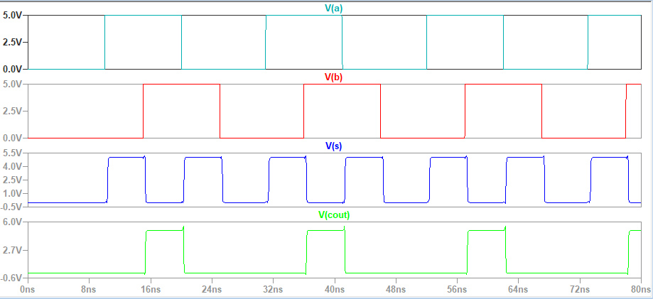
Figure
2:Simulation on xor gate.
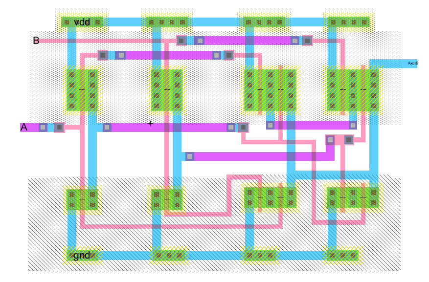
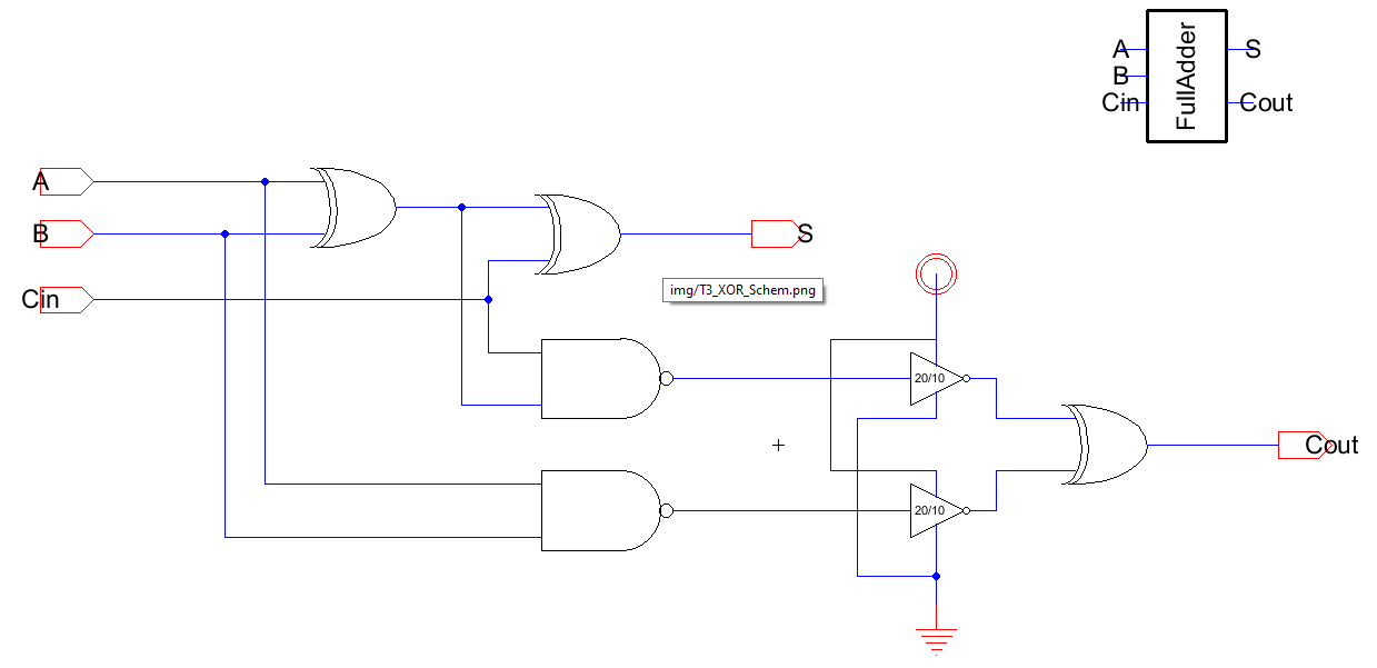
The layout of the xor gate was then created.
Figure 3: Layout view of the xor gate.
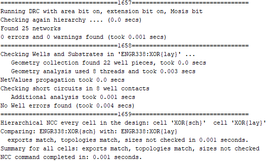
ERC, DRC, and NCC were also checked.
Figure 4: Checking for errors.
Task 4: Create Schematic and Layout of Full Adder
The schematic of the full adder was first created and simulated
Figure 5: Schematic view of the full adder.
The schematic was then simulated in LTspice.
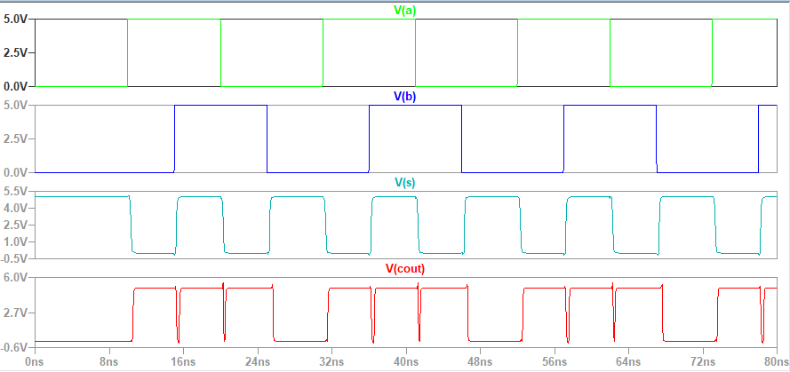
Figure
2:Simulation on full adder.
The layout of the full adder was then created.
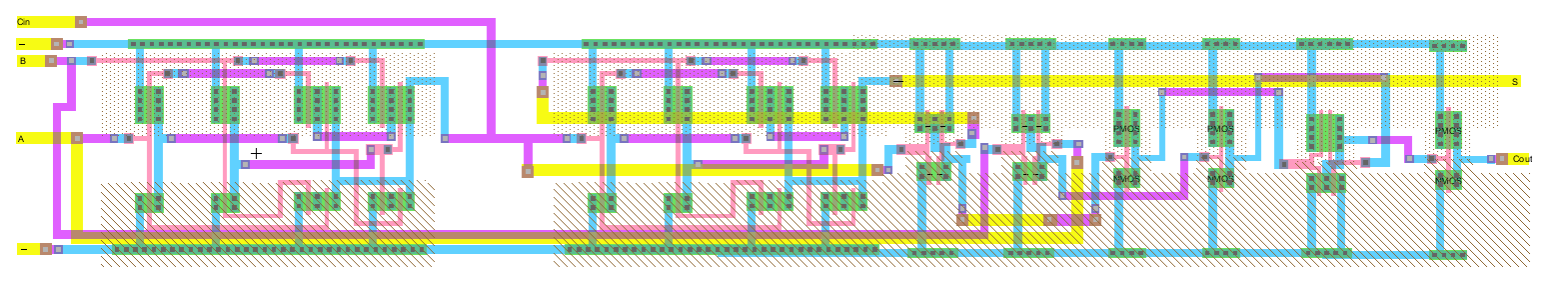
Figure 3: Layout view of the full adder.
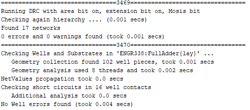
ERC, DRC, and NCC were also checked.
Figure 4: Checking for errors.
Discussion:
This lab detailed the design and simulation of a transistor level
logic gates, AOI logic, and a full adder. Schematics, layouts, and
error checking tools were also included.