ENGR337 Lab 2020 Spring
Project
Name: Humberto
Arredondo Perez
Email:
harredondoperez@fortlewis.edu
1. Title: Final Chip Layout
2. Introduction
The goal of this lab was to wrap up the final chip layout using al the
componentsthat we design over this tutorials using ElectrcVLSI.
3. Materials and Methods
In
this lab we built an Op Amp and analized its bihavior using a bias and
a set of transistors for the gain. we also used a software call
ElectricVLSI and the tutorial 5 given
by
DR Li to finally wrap up the final layout for the design of a chip.
First we created the op amp, we created the bias, and a set of
transistors that gave us the gain. At the same time we created a
schematic of this chip an we checked for errors.
4. Results
In figure 1,the open loop gain of the op amp using a resistor off 300k
was found that increase the gain the most compare to the other ones. In figure 2, we have the Vout-gain divided by
our Vin, and we can see the goin right at the bottom of the jump. The
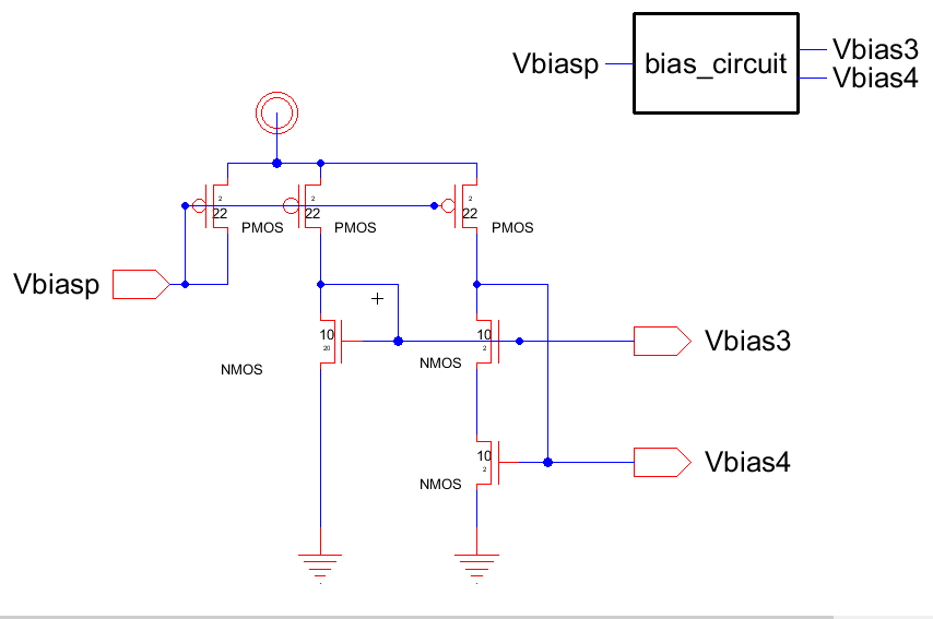
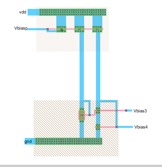
bias was created in a schematic and in a layout (Figure 3), like wise,
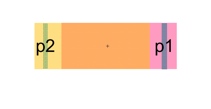
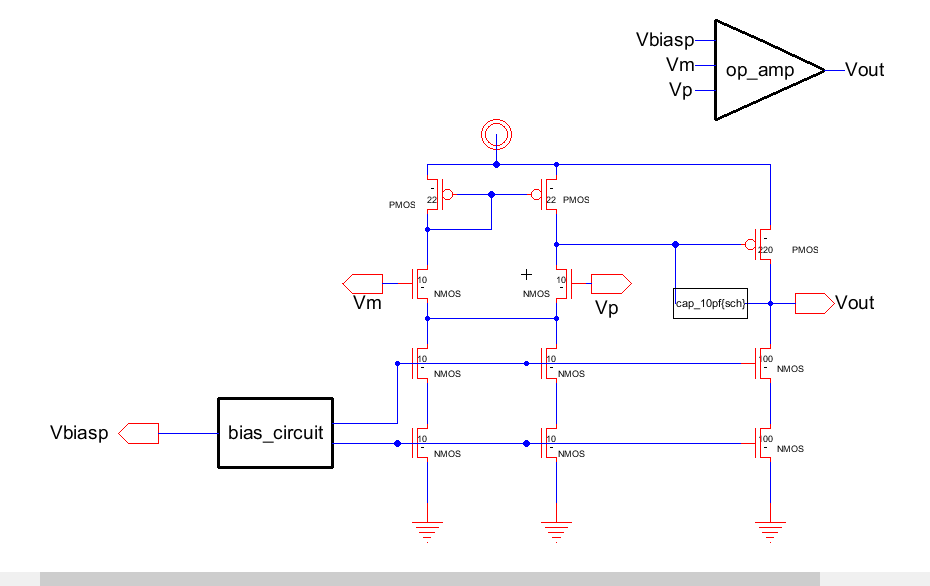
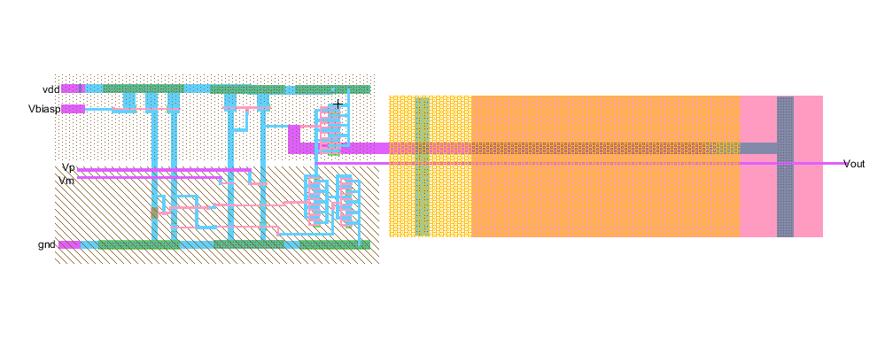
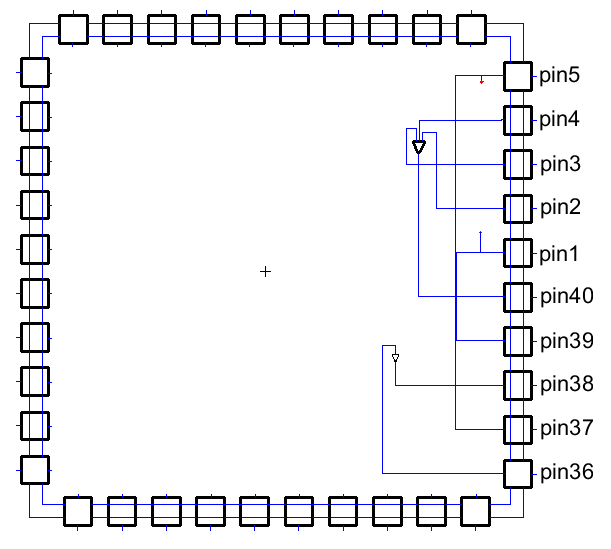
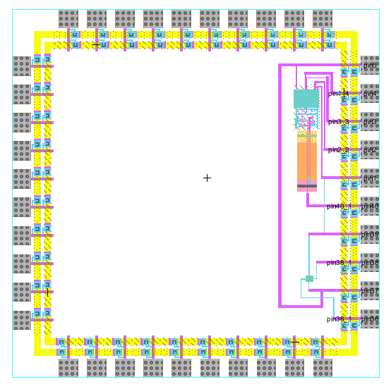
the cap (Figure 4) an the op amp (Figure 5). the final chip schematic
and layout are shown in Figure 6 and 7 respectively.
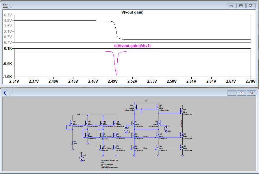
Figure 1. Open loop
gain in our Op Amp.
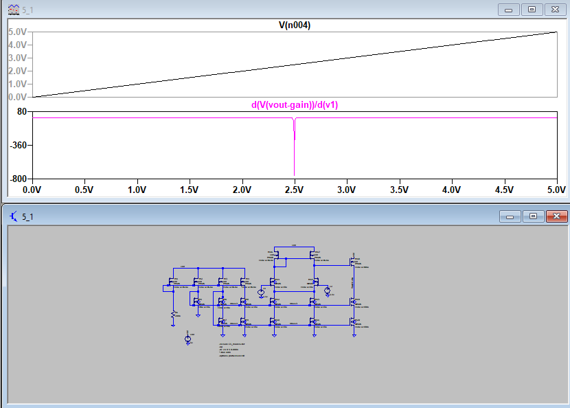
Figure 2. Vout-gain / Vin
simulation.
Figure 3. Bias schematic and
layout.
Figure 4. Cap schematic and layout.
Figure 5. Op Amp schematic and layout.
Figure 6. Chip schematic and
layout.
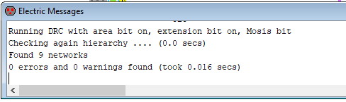
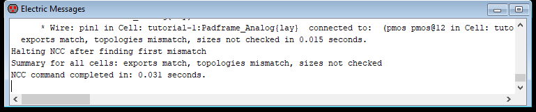
Figure 7. Check for errors and mismatch.
5. Discussion.
In this lab we disigned an Op Amp simulation in LTSpice,
we found out how the gain changes with different resistor values,
and prove the operation points of the transistors. The chip Layout was
finally compleated after some issues. In this project we were
able to have a clean DRC (F5), but we were not succesfull on NCC
matching our topologies. Over all, a great experiance creating this
small chip while learnig a new software.