ENGR337 Lab 2020 Spring
Lab 9
Name: Humberto
Arredondo Perez
Email:
harredondoperez@fortlewis.edu
1. Title: Layout The Padframe
2. Introduction
The goal of this lab was to learn how to layout the padframe for a chip with ESD (electrostatic discharge protection).
3. Materials and Methods
In
this lab we used a software call ElectricVLSI and the tutorial 4 given
by
DR Li to create a padframe for the design of a chip. First we created
two diodes, NMOS and PMOS diodes, in a way that they will be protected
form a overheating situation. These diodes are connect with a wire in a
passivation layer that concists of two analog oins, two ground pins and
to power pins for a total of 6. An icon was created and a layout and
schematic padframe were also created using an Array all the way around
a square shape. After every step the layout and schematic were checked
up for errors.
4. Results
In figure 1,the schematic of the inverter with NMOS and PMOS
transistors are showen after
were modified in terms of lenght and names of dimentions
and place a code. In Figure 2 the results of figure 1 are showed from
LTSpice. Then we are showing on Figure 3 the layout version of this
inverter.
Figure 4 We have the simmulations of Figure 3 squematics
and with the respective code to make them work.
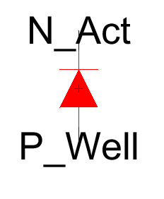
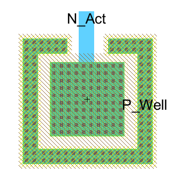
Figure 1. The N_Act - P_Well diode schematic and layout.
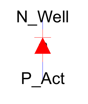
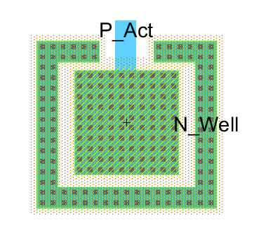
Figure 2. The P_Act - N_Well diode schematic and layout.
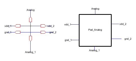
Figure 3. Pad Icon and Pad layout.
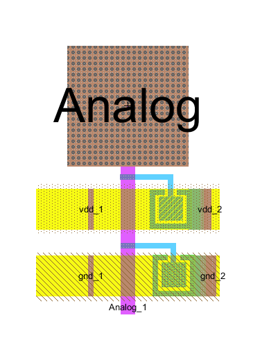
Figure 4. The Pad layout.
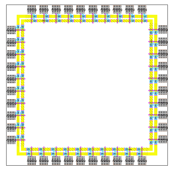
Figure 5. Padframe layout.
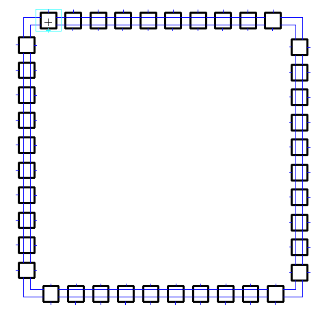
Figure 6. Padframe schematic.
5. Discussion.
In this lab we disigned
a couple diodes, Icons and Padframe for a chip with ESD protection ring.
Lab of
this series of 5 in total. checking for errors its a powerful tool and
time saver when disigning on ElectricVLSI. This lab is been the most
time consuming one, due to a requirement of big attention to every wire
we connected, and finding to debug the errors in the whole process.