ENGR337 Lab 2020 Spring
Lab 7
Name: Humberto
Arredondo Perez
Email:
harredondoperez@fortlewis.edu
1. Title: MOSFET's and IV Curves
2. Introduction
The goal of this lab was to learn how to
design a layout for a NMOS IV and PMOS IV in ElectricVLSI by
following the instructions of the tutorial 2.
3. Materials and Methods
In
this lab we used a software call ElectricVLSI and the tutorial given by
DR Li. We created a new cell for the NMOS and PMOS node that we
designed, we changed the length, labeled the nodes and simulates the
currents in LT Spice, we dod this for both nodes in schematic and
layout. We learned how to check for erros annd adressed them.
4. Results
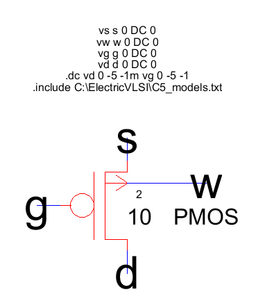
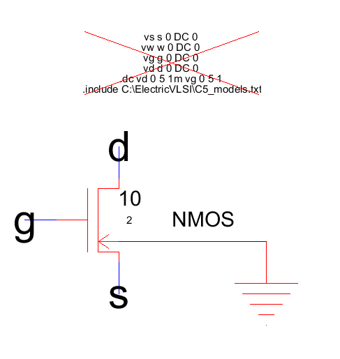
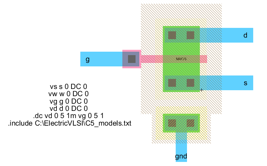
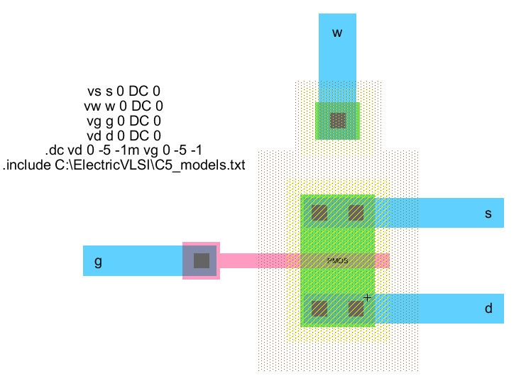
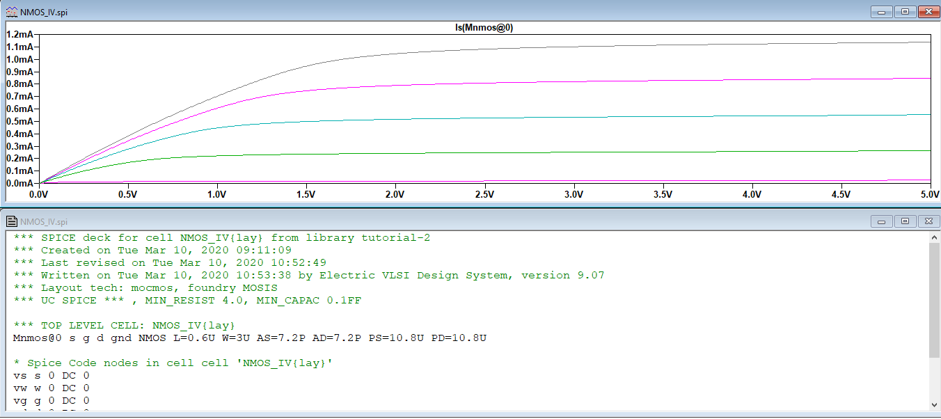
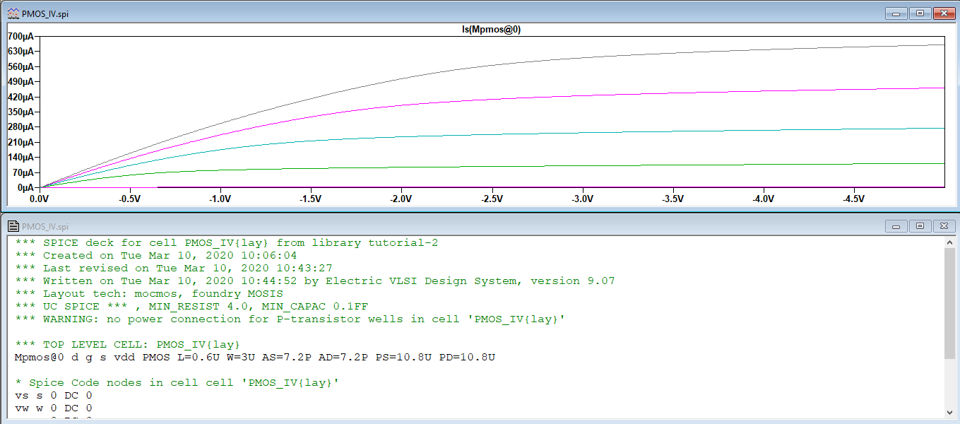
In figure the schematic of the nodes of NMOS and PMOS are showen after were modified in terms of lenght and names of dimantions, then we are showing on Figure 2 the layout version of this two nodes.
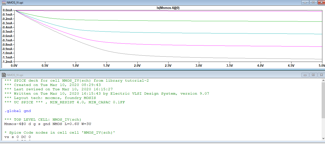
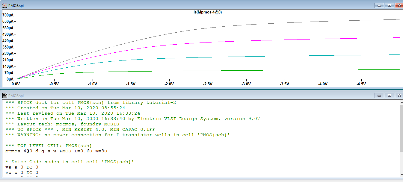
Figure 3 We have the simmulations of the nodes in Figure 1 squematics and with the respective code to make them work.
Figure 1 NMOS and PMOS nodes with code.
Figure 2 Lay out of NMOS and PMOS with code.
Figure 3 Squematics in Spice of using that scode showed respectively.
Figure 4 Layouts ran in Spice with the code showned
5. Discussion.
In this lab we
got
designed a MOSFET's and thier respectively IV Curve, lernded how to
labaled, sized, check for errors, run on Spice. Great second lab of
this series of 6 in total. We found out that if we check the schematic
and the layout for mistakes at a goog rate of progression during
design, we can avoid headache in the future when it comes down to
debuging the whole system.