3. Procedure
For this lab, we created our 1A circuit by following the schematic of a common DC-DC voltage converting circuit. The circuit we used for reference is shown below:
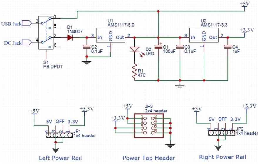
For our purposes, the left and right power rails and the power tap headers were left off so that we could later add our own that fits our purposes better.
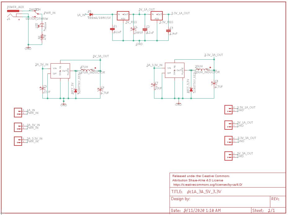
For the 3A circuits, we followed the schematics, provided by Texas Instruments, of circuits commonly used with the LM2596 voltage regulators they make. We followed one for a 5V 3A output with an input range of 7-40V.
We also followed one for 3.3V 3A output with the same input range.
Finally, we added 3 male header-pin pairs for shorting the different input options, and 4 pairs of female header pins, one pair for each output option. Once this was done, we designed the necessary libraries for the components we are using.
Libraries were created only if they were not already found in the SparkFun Eagle libraries. After the schematics were drawn in Eagle, we began to format the physical layout of the PCB itself.
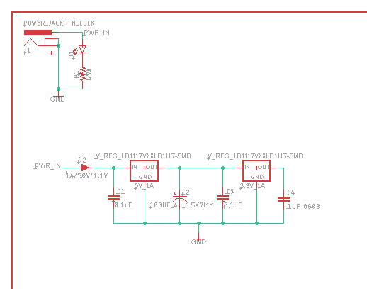
The schematic with just the 1A circuit:
The schematic with both 5V/3V 3A circuits, the 5V/3.3V 1A circuit, and the headers.
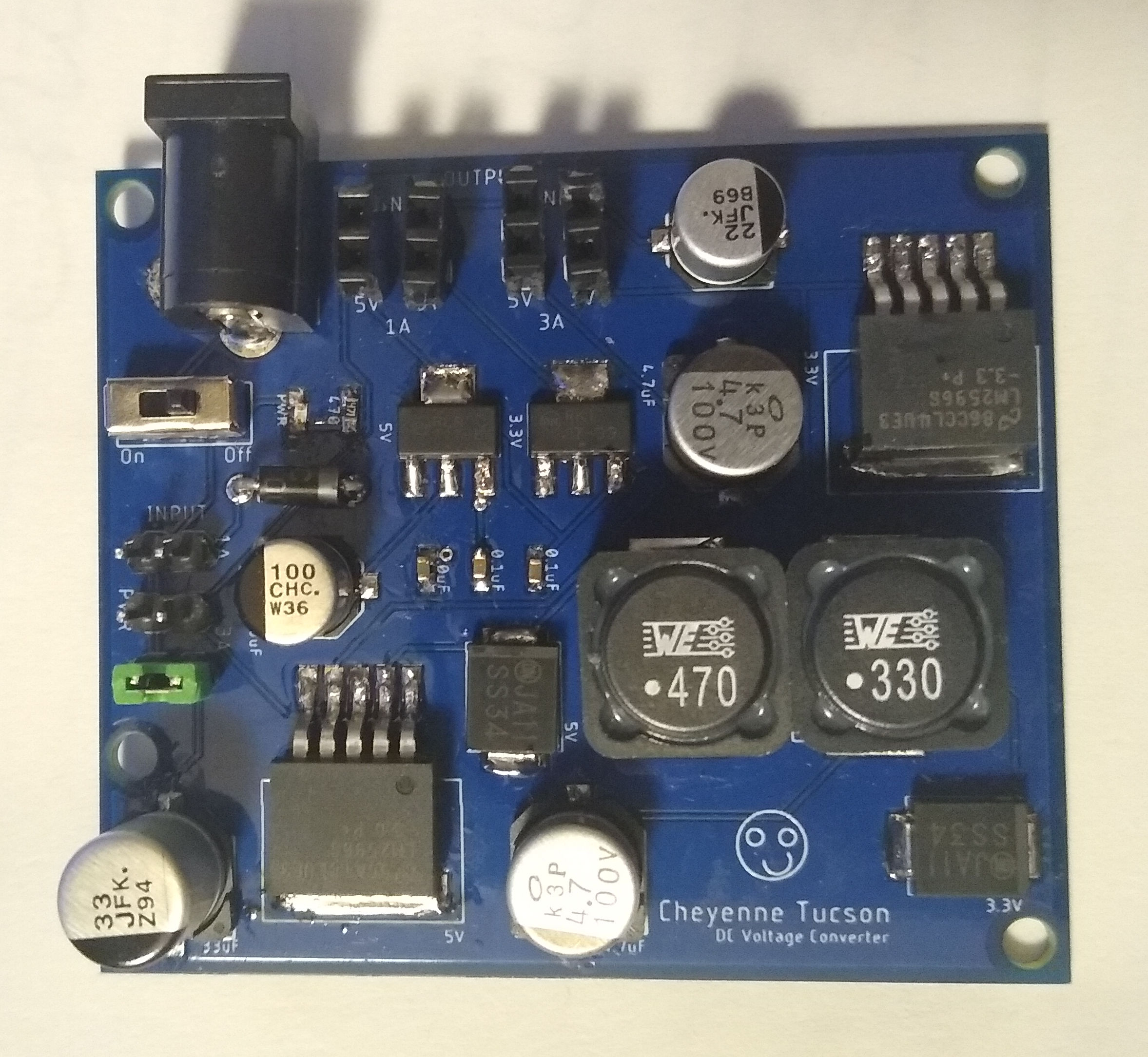
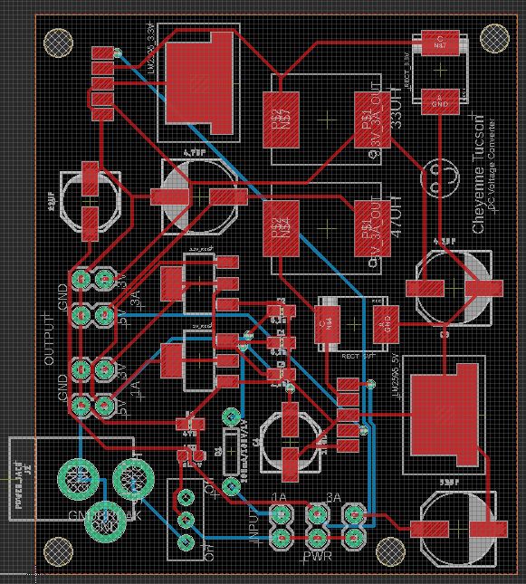
The PCB layout of both the 1A and 3A circuits
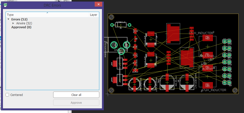
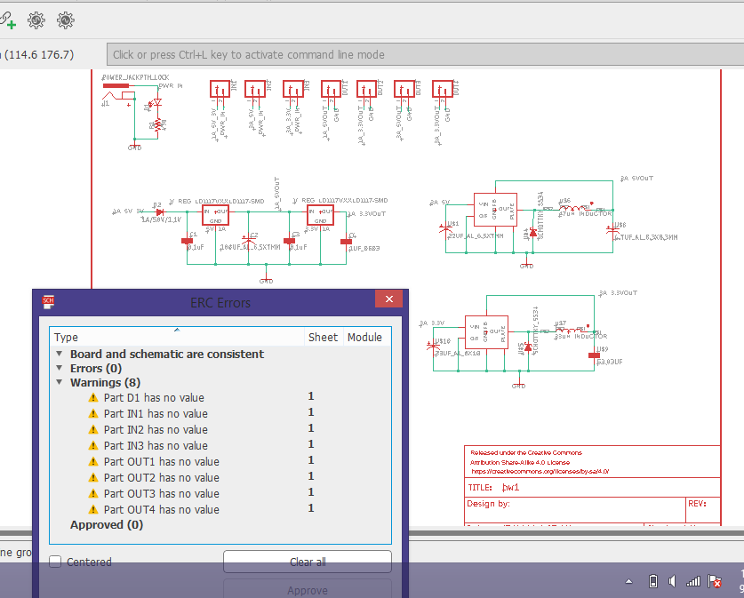
Checking for errors with the DRC and ERC:
The libraries and project files can be found here.
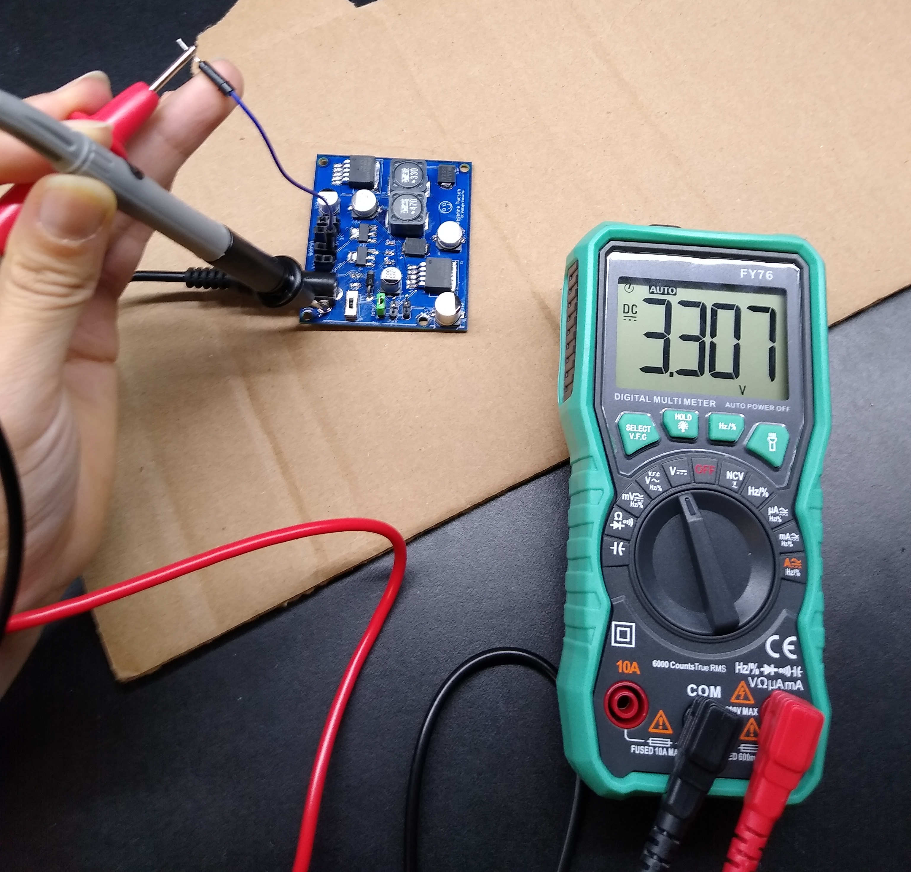
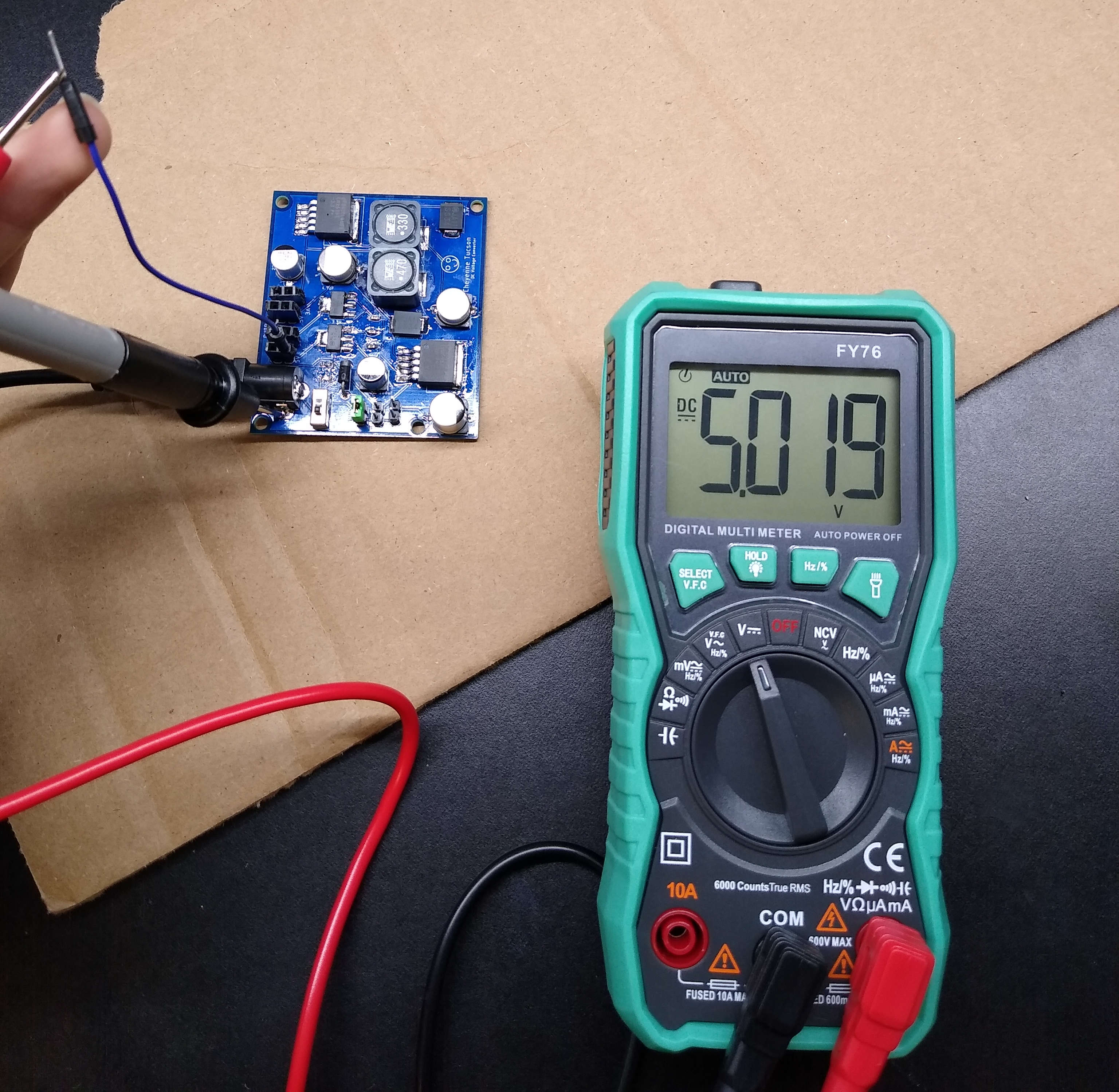
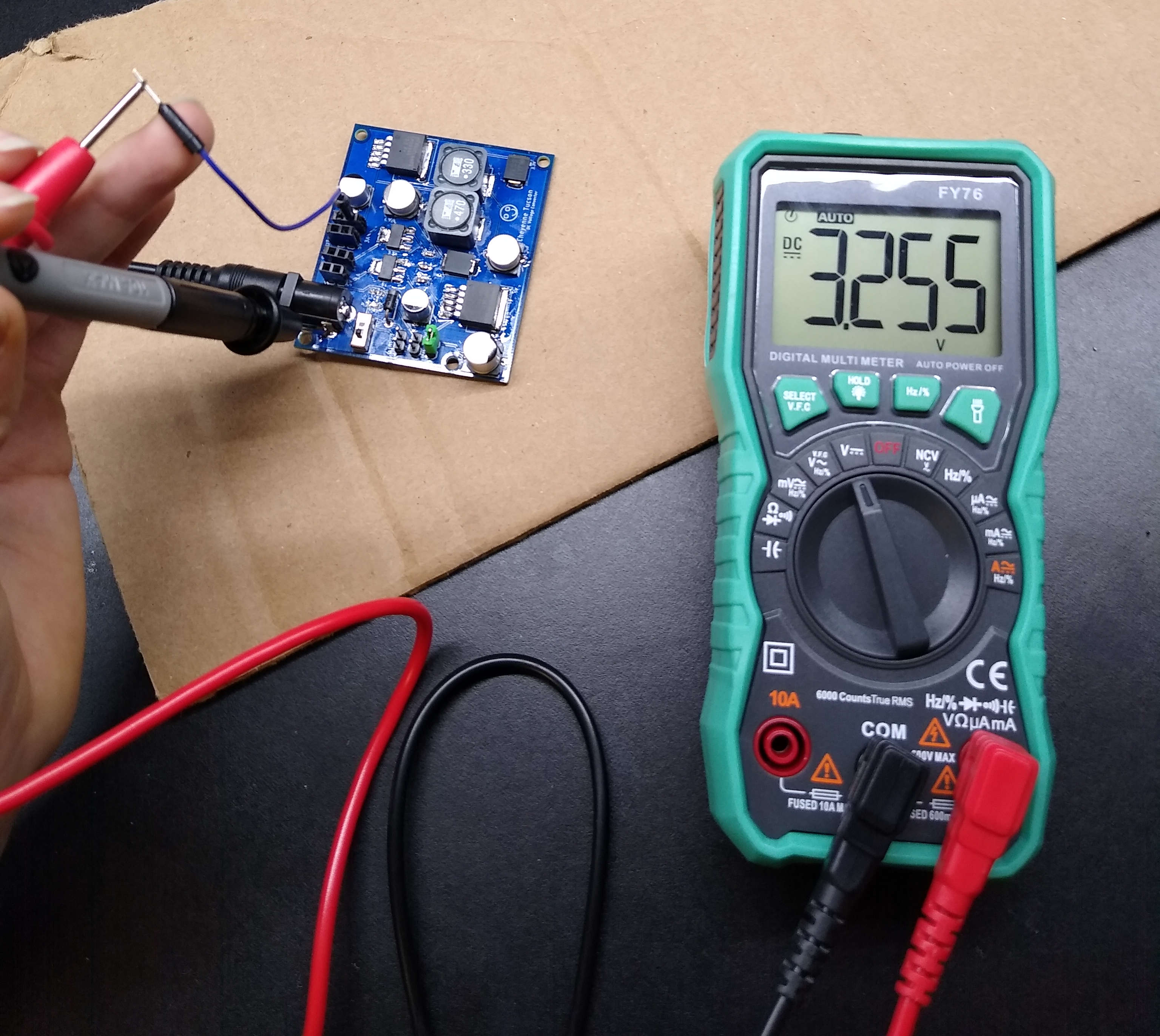
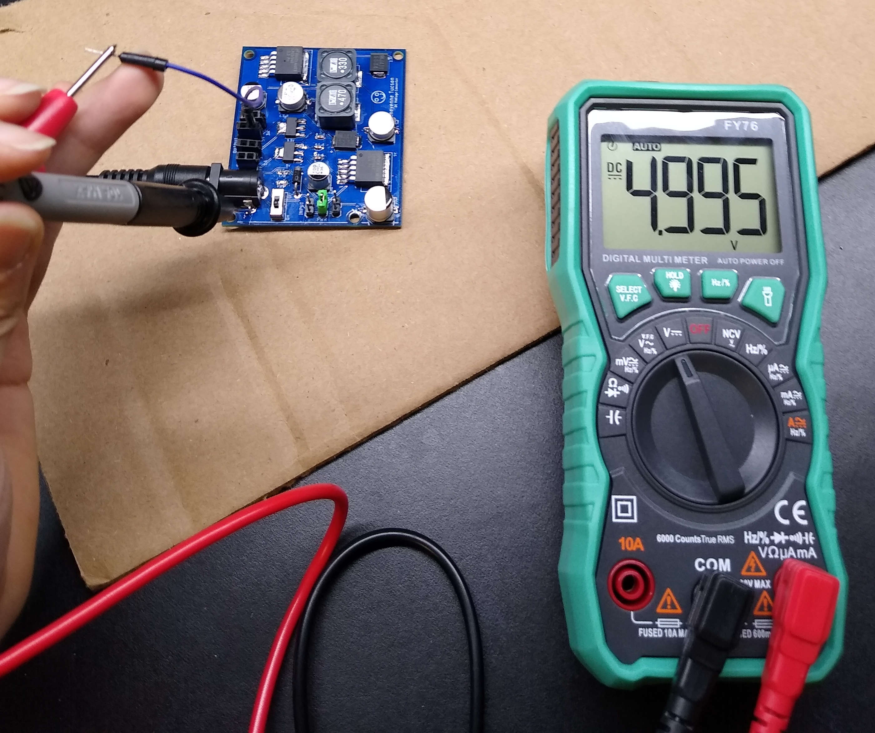
4. Results