ENGR338
Digital Electronics Course Project - An 8-bit SAR ADC
In the Spring 2021 semester,
you only need to build the 8-bit SAR block
and simulate it in LTSpice to show its functionality. Report the
simulation results of the 3-input NAND gates, the TI DFF, and the 8-bit
SAR block for credits.
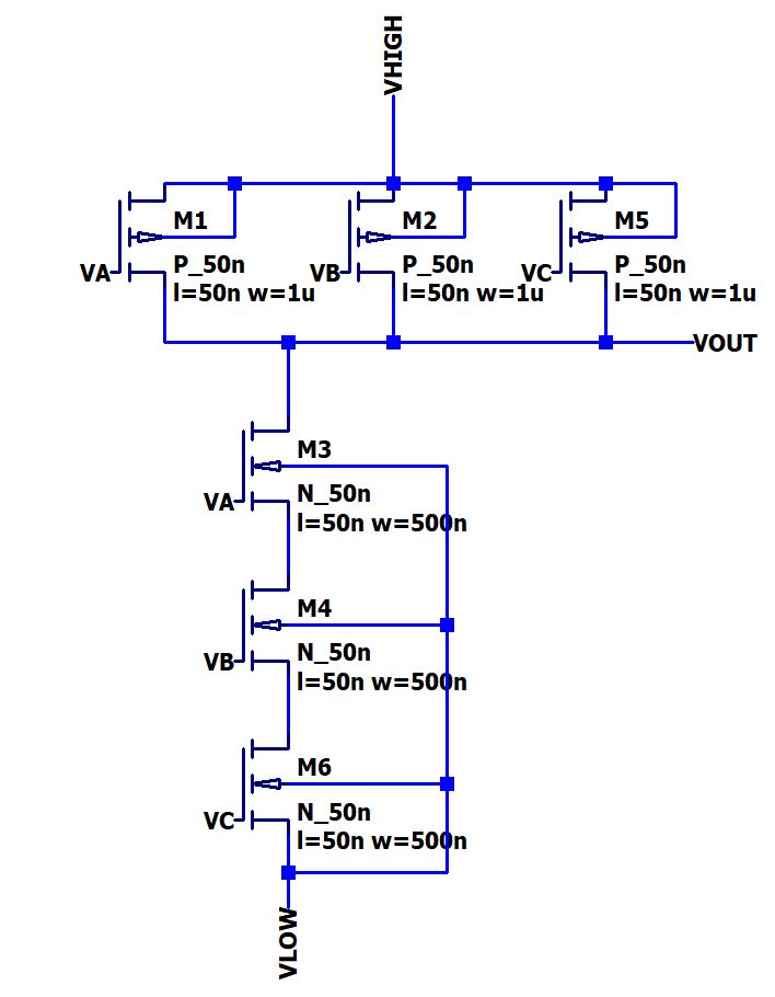
The 3-input NAND gate:
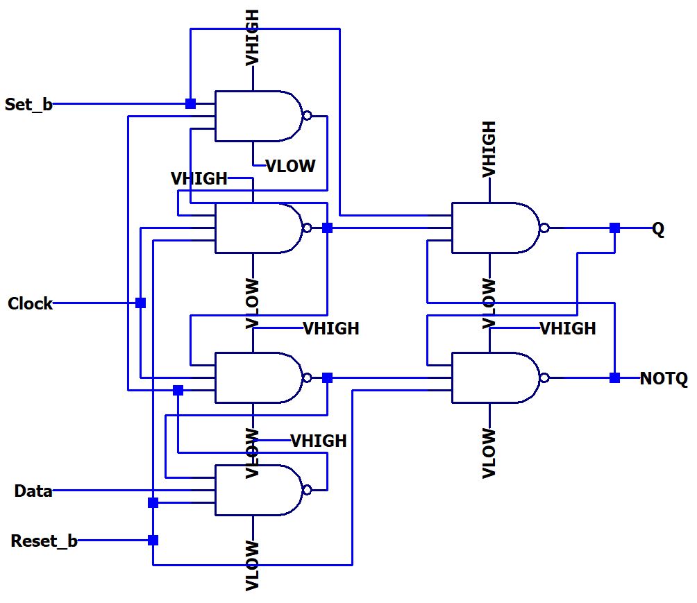
The TI DFF:
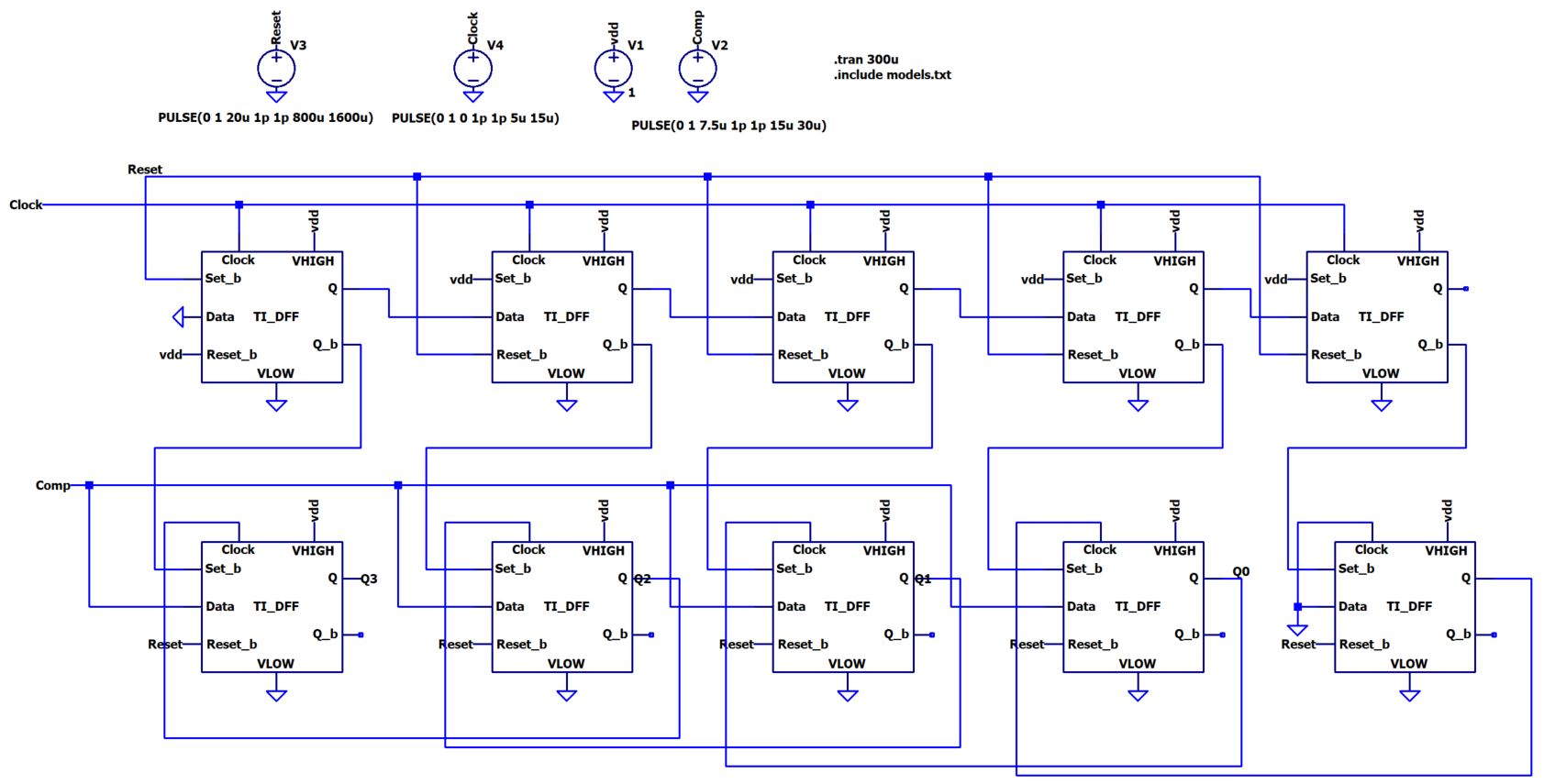
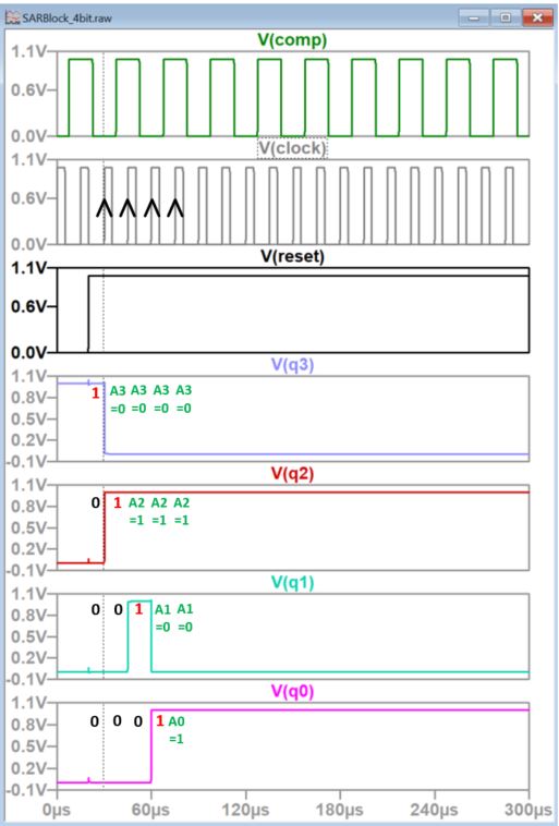
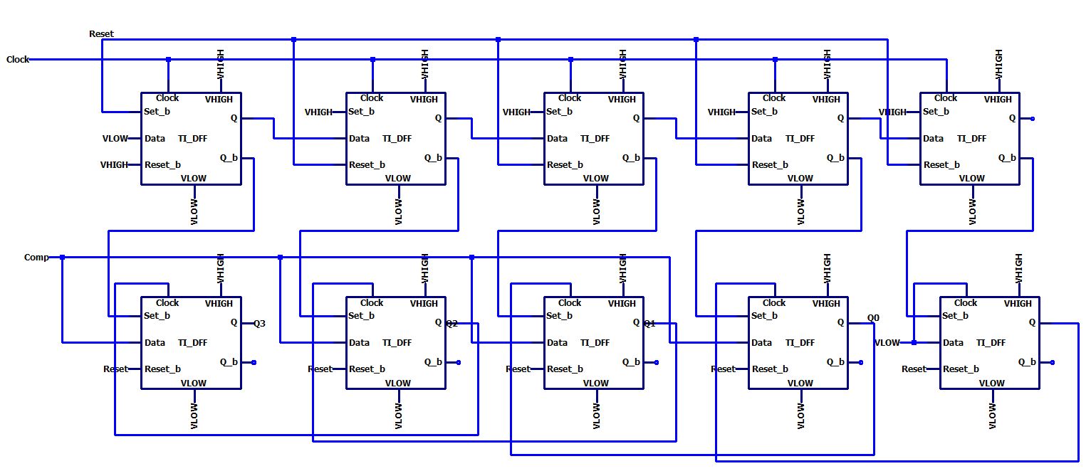
A 4-bit SAR block was built
and simulated. The following simulation
shows the Comp values (intermediate digital outputs) are ready at the
output at the 5th clock rising
edge.

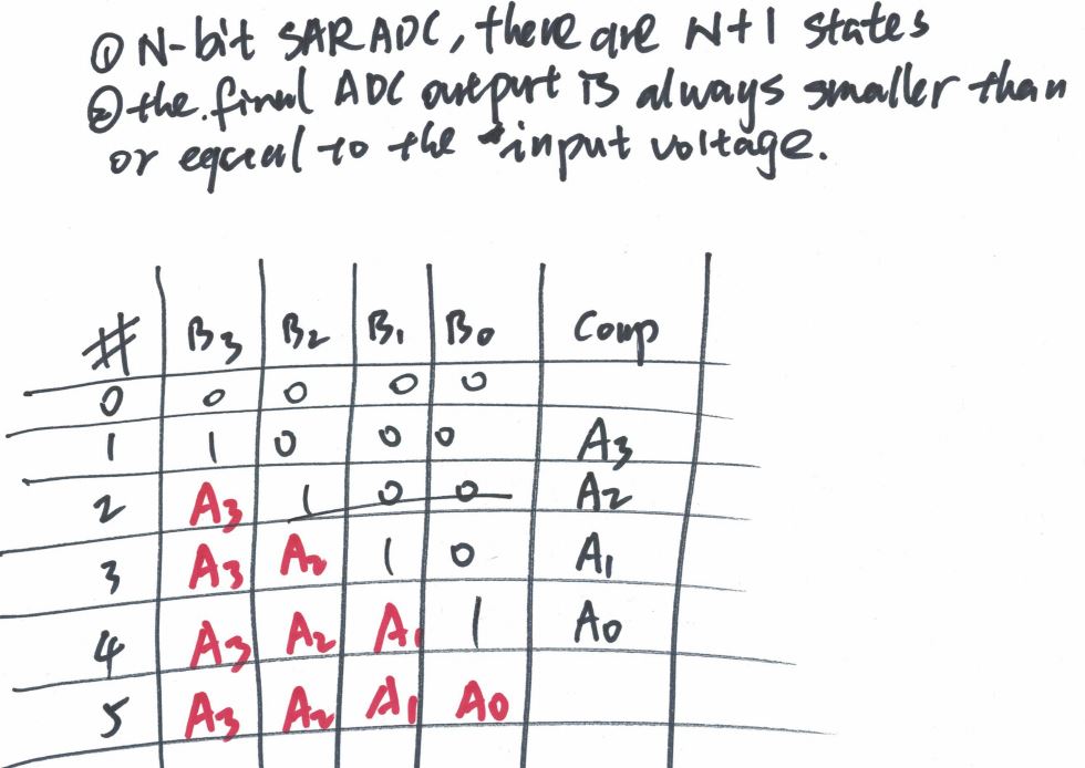
A snippet from the lecture
notes:
The final simulation
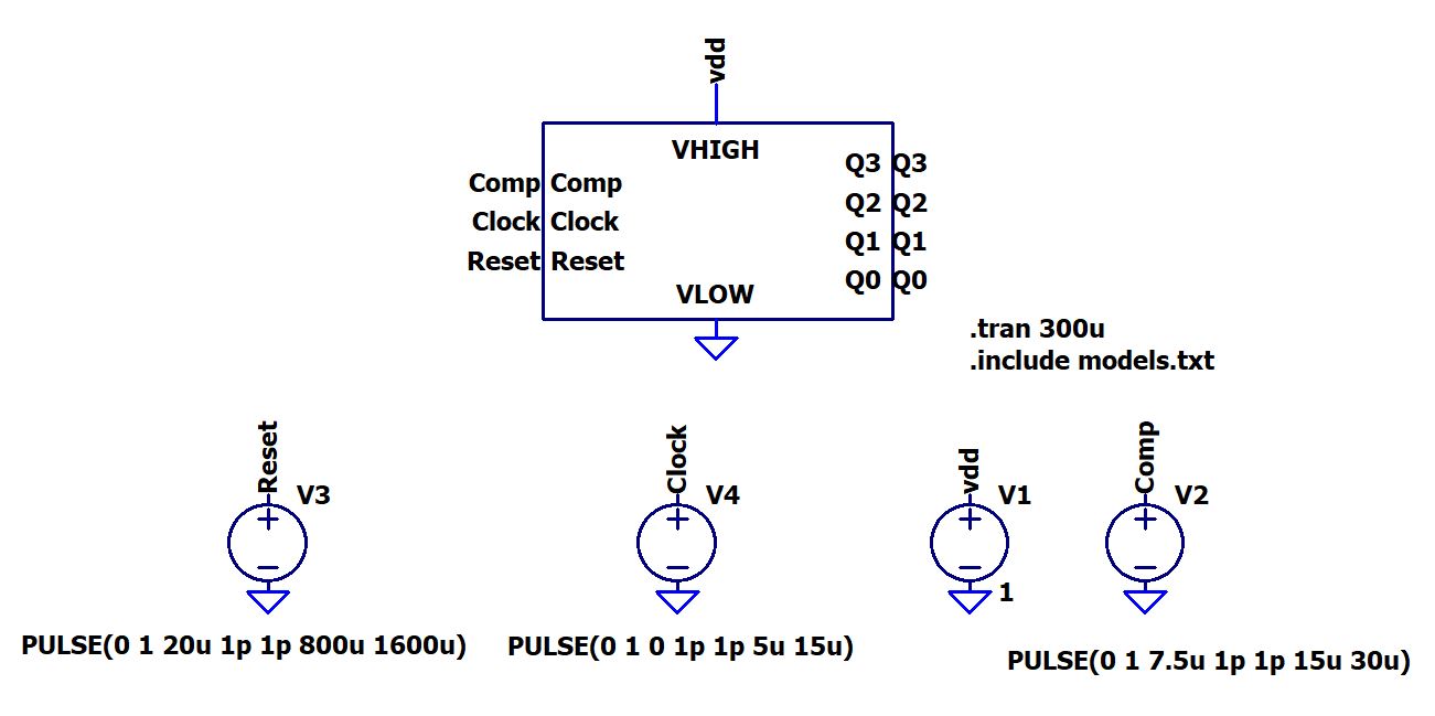
schematic should use a symbol of the 8-bit SAR block. The example of
the 4-bit one is shown below:
(You must delete all the
voltage sources and leave the pins available for the upper level symbol)
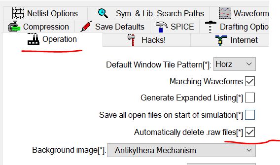
In order to delete the .raw,
.plt, .net, and .log files, go to Control Panel - Operation, check the
box of 'Automatically delete .raw files'.
Upload the report to the lab report website by 5 pm on the due date.
Grading rubric:
1. NAND gate simulation (25 points)
2. DFF simulation (25 points)
3. SAR simulation (25 points)
4. Report writing (25 points)
Do not send this to my email, upload the report as a normal lab report on the website
Refereces:
TI DFF
Sample/Hold
Cricuit in LTSpice
The comparator is provided.
Use the circuit in Figure
24.61 in Dr. Baker's CMOS book.
The
columbia VLSI desgin lab.
Abo's 1999 paper.
SAR ADC lecture video and notes
Berkeley
EE247 ADC interfaces, including Charge Scaling DAC,
Slides