ENGR338
Digital Electronics Course Project - An 8-bit SAR ADC
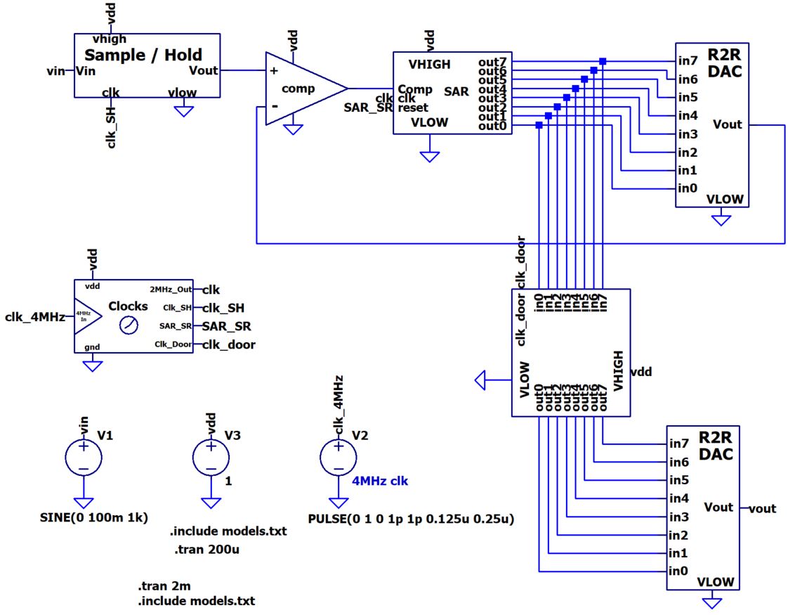
1. System overview
This SAR ADC uses the 50nm technology from our textbook - CMOS Circuit
Design by Dr. Jacob Baker. The entire LTSpice folder which includes the
model file can be downloaded here.
The system diagram is shown below.
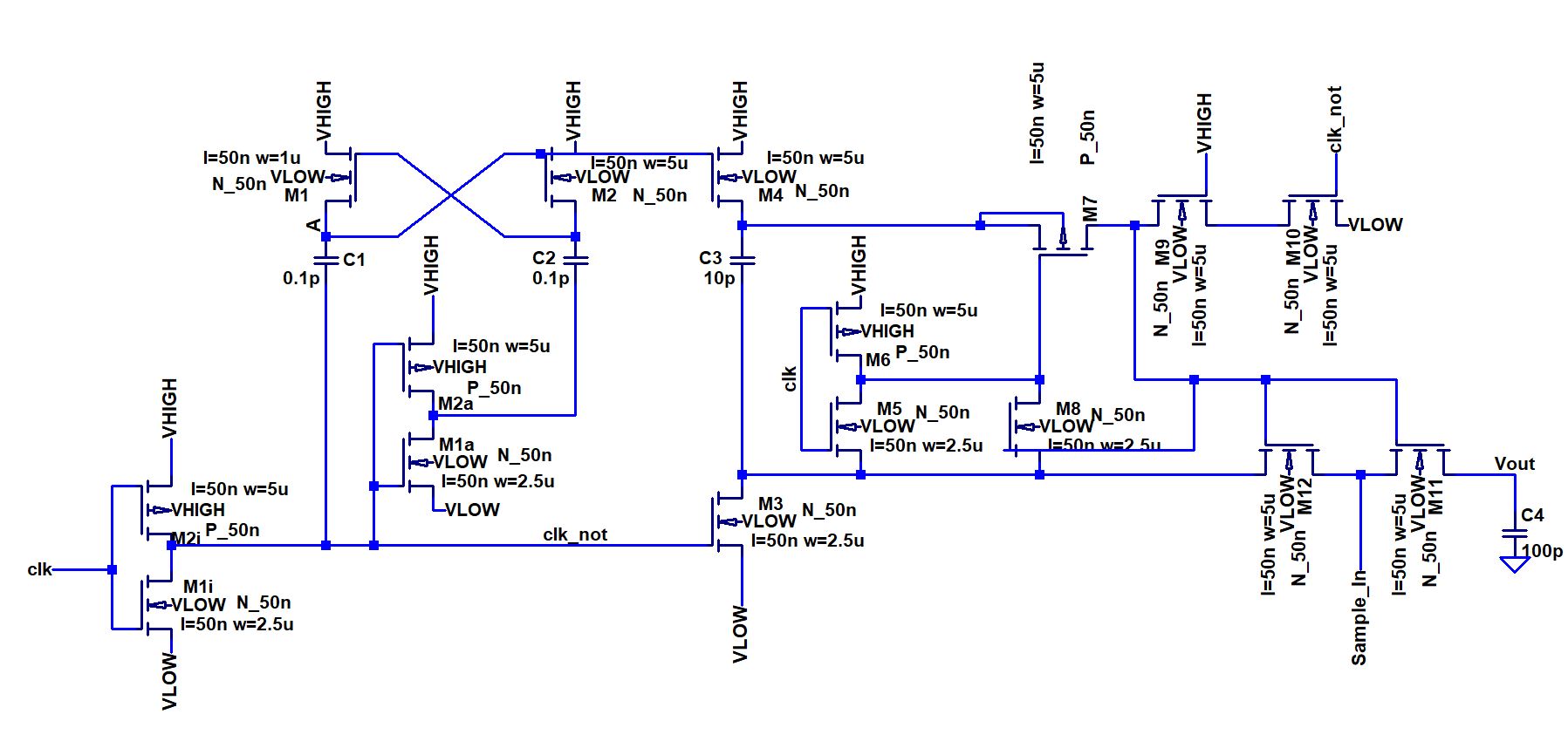
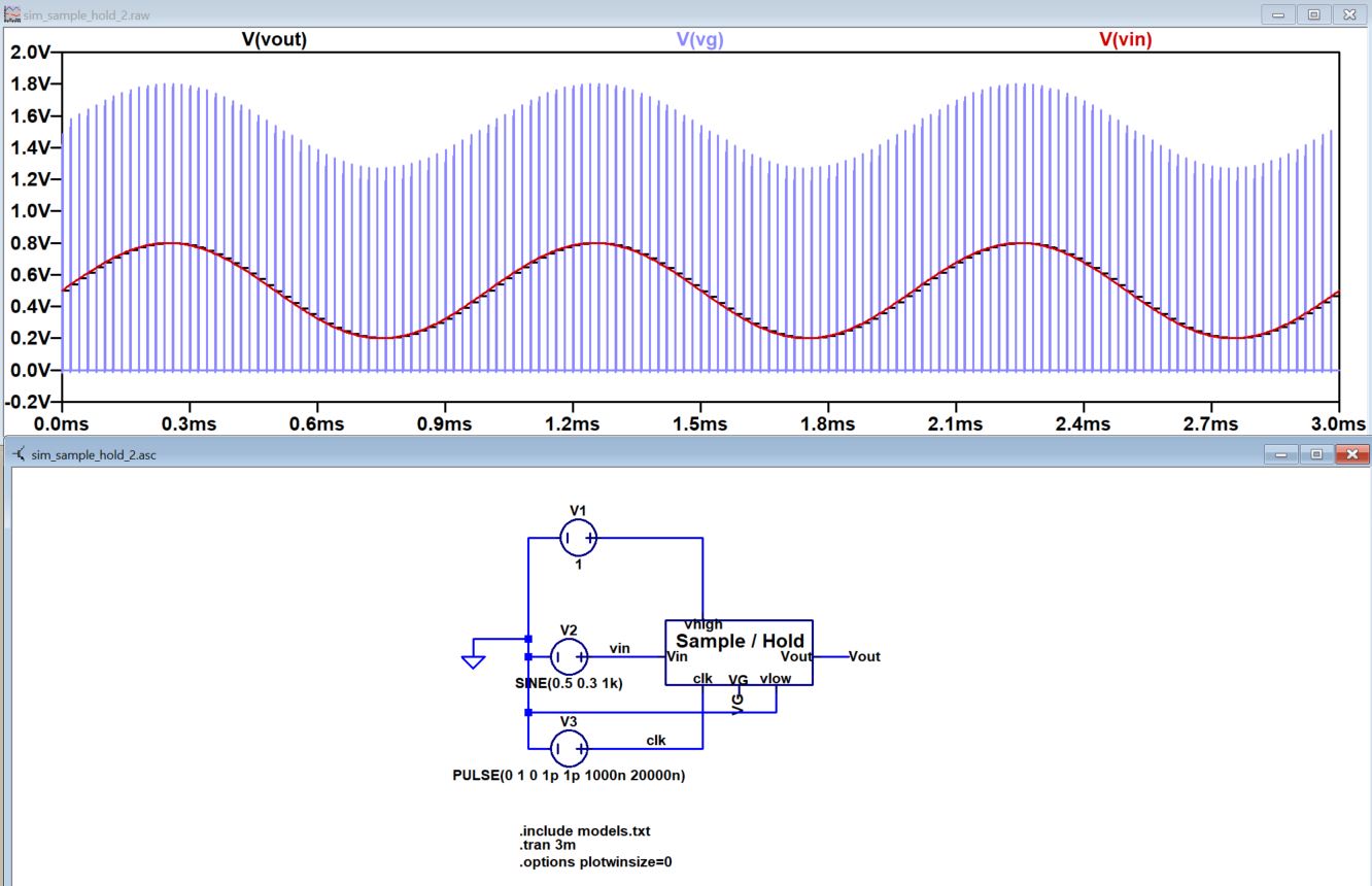
2. The sample and hold circuit
The sample and hold circuit was published by Abo et al in 1999 (Abo's 1999 paper)
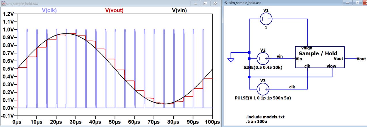
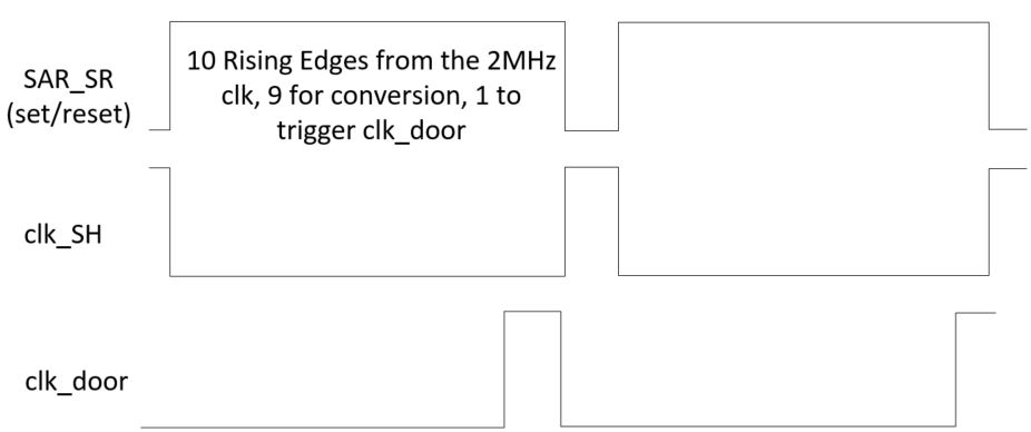
Please note that it is ok to use 50% duty cycle clock to run the
sample and hold circuit. However, the AD conversion only happens during
the 'holding' period, so the sample/track time only needs to be just
adequate to acquire the analog value and then give the rest of time to the
'holding' state. In the following simulation you can tell that the duty cycle is < 20%.
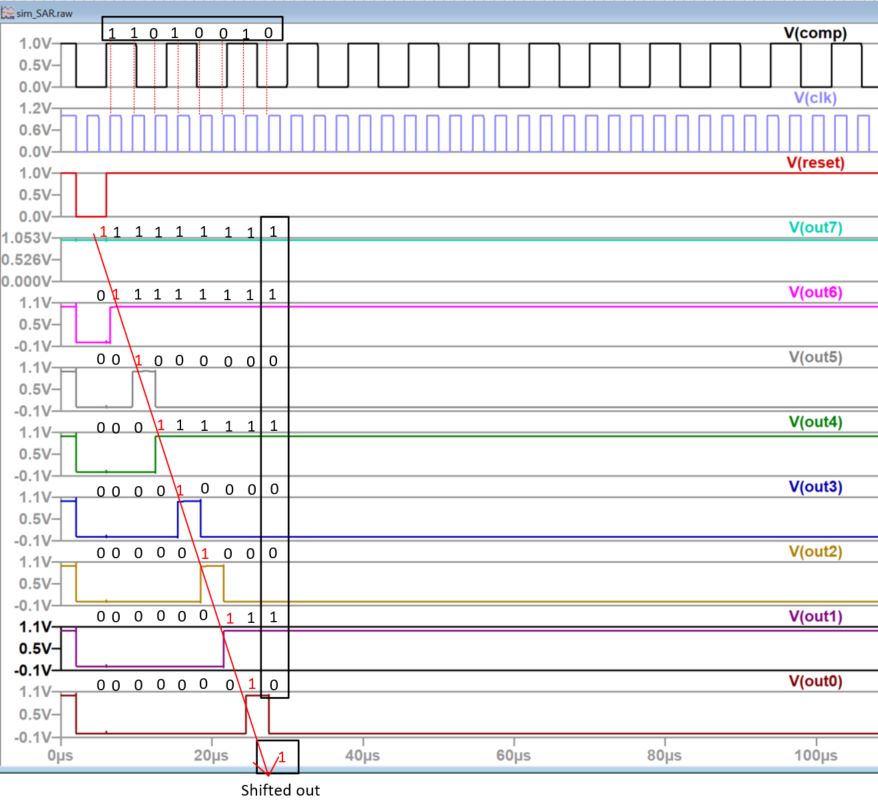
During the 'holding' period, the 8-bit SAR ADC runs the data conversion
which requires 10 rising edges. 9 for the 9 states to complete the SAR
algorithm, the last is to send the data out.
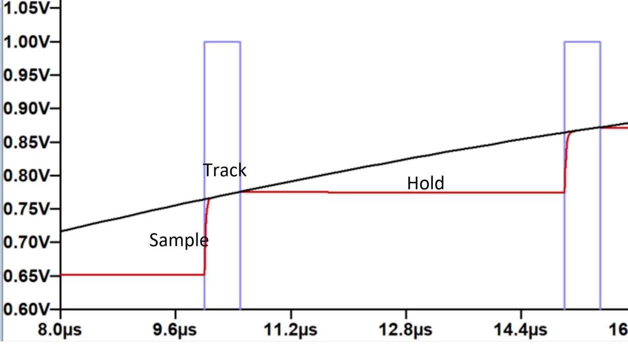
If you probe VG, you will find that VG is tracking the input signal:
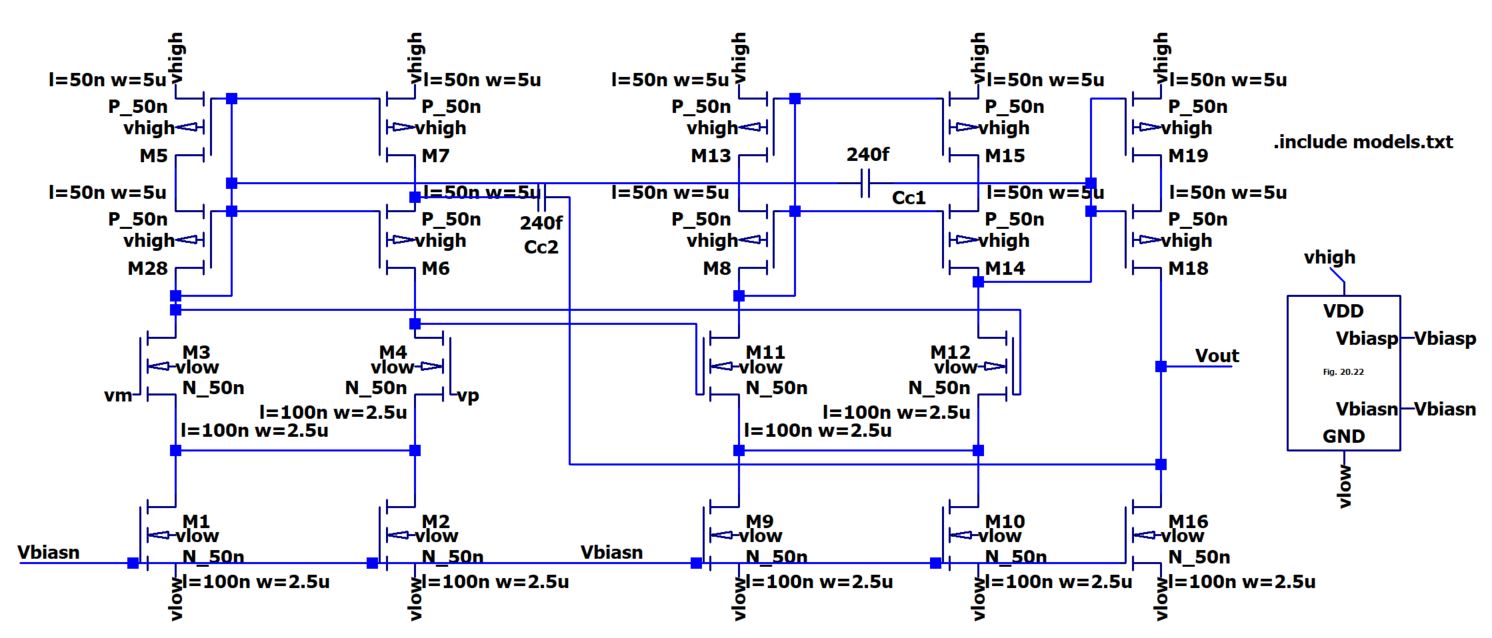
3. The operational amplifier
The op amp circuit came from Dr. Baker's textbook (Figure
24.61). Please note that the biasing circuit is usually not shown in the op amp's circuit.
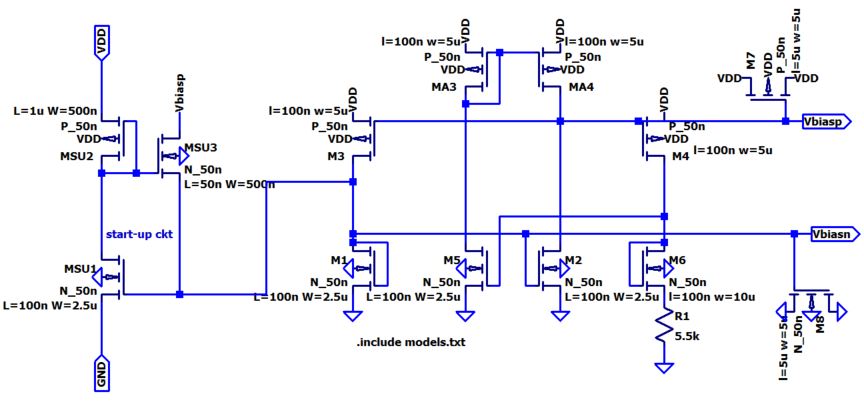
The schematic of the biasing circuit
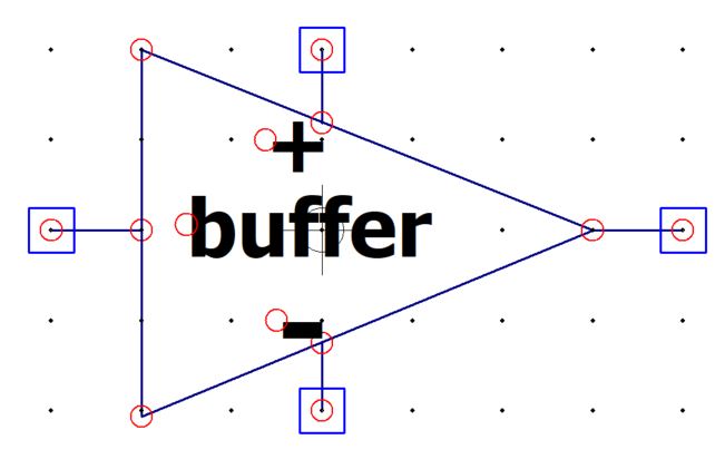
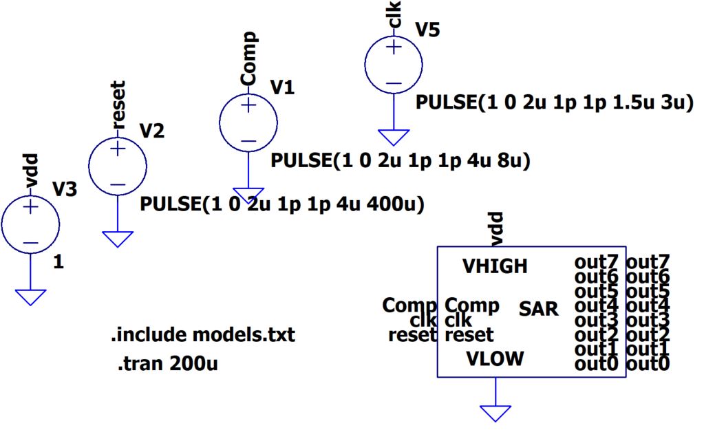
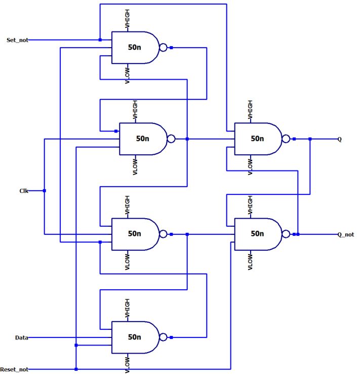
4. The SAR block
No magic here. As a pure digital circuit, it just operates as expected.
The triangle shape parts are buffers which strengthens the driving
capability of the clock. It may not be very necessary for the
simulation but it helps the real circuit since there are many stages in
which every stage contributes a capacitive load.
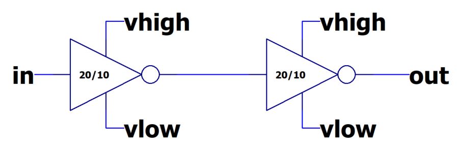
(Figure credit: Audra Benally)
In your report, you must show the simulation results of the SAR block to demonstrate that it implements the SAR algorithm.
5. The R-2R ladder DAC
In this project, you need to use the same DAC twice. One is used
inside the SAR ADC system, the other one is used to conver the overall
digital output into an analog signal so you can probe it and show it in
one single plot pane in LTSpice.
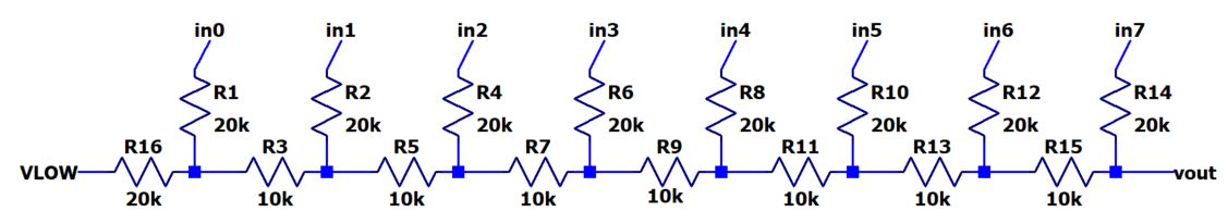
(Figure credit: Audra Benally)
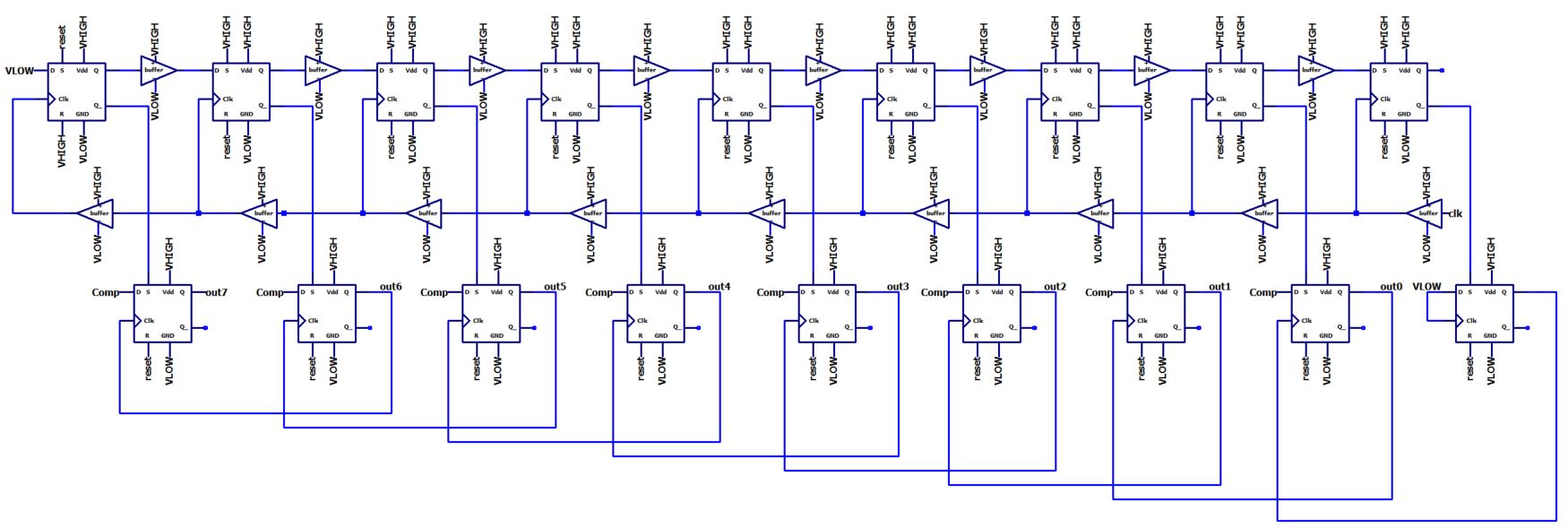
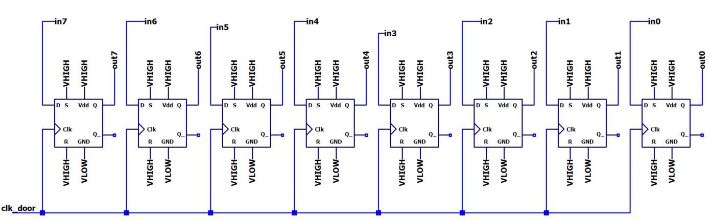
6. The timing block and the 'door' register
Understand and implement the timing of the SAR ADC takes 80% of the
effort in the overall design. You must know what the circuit does at
which time period to design the circuit.
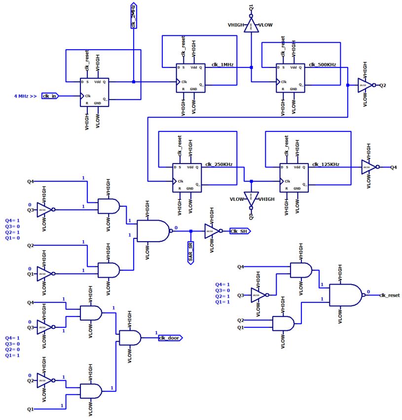
(Figure credit: Audra Benally)
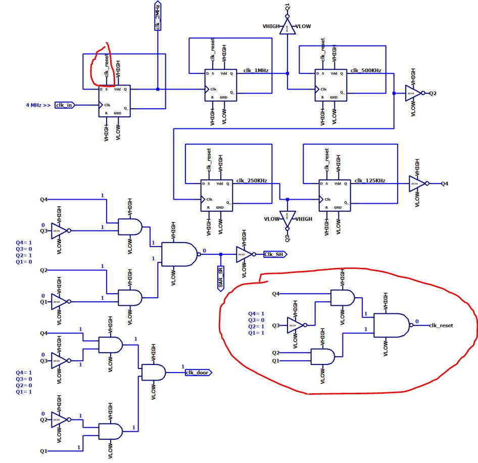
There is a signal 'clk_reset' in the timing block. It is triggered when
the 2MHz clock counts to 11. It clears out the counts in the counters.
For the TI DFF used here, when the clk signal is 0, the FF holds the
current value, so for the 11th count, the output of SAR shouldn't be
affected. However, the counter clears itself once it hits the designed
maximum count, please try to not use this 11th count from the clk_reset pin and report the resutls.
The TI DFF holds the previous values when clk is 0.
The 'door' register is very simple:
7. Two observations (answer these questions in your report)
Question 1:
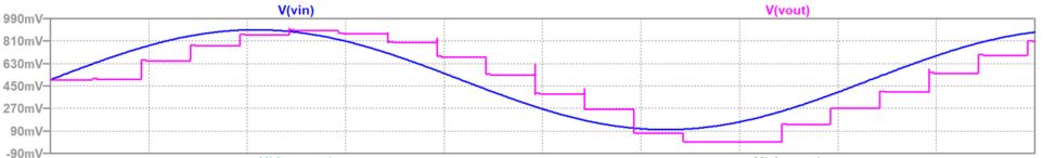
From the example report drafted by Audra, there is a figure that shows the vin/vout of the ADC:
I simulated my circuit and shows the following result (it took me over 1 hour to complete this simulation on a core i7 HP Zbook)
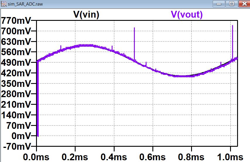
Zoom-in view:
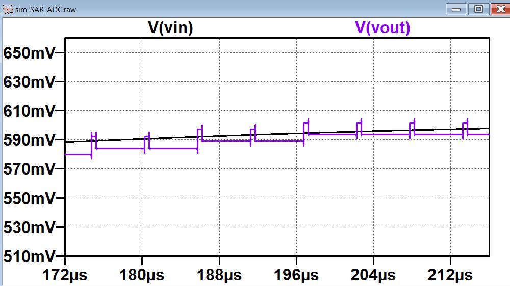
Why they look so different? Does that mean the resolution of Audra's ADC is inferior to mine?
Question 2:
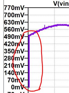
There is a huge dip at the very beginning of the output. Does that mean
the ADC fails converting the input into a digital signal so it is
useless?
Question 3:
If you probe the output signal from the sample and hold circuit, it shows the folloing result as V(n002):
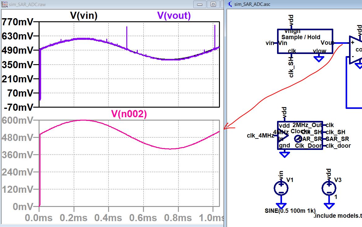
It looks exactly the same as Vout so why do we bother having all the
other circuit blocks following the S/H circuit for the conversion to
get Vout? Why not just use V(n002)?
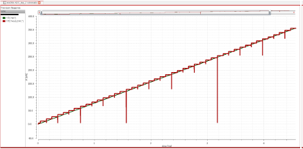
8. What are the INLs and DNLs of this ADC?
You can run a DC sweep of the input and probe the output stair
response. Export the data from LTSpice, and use Matlab to calculate the
DNLs and INLs.
The following simulation figure is from the the
columbia VLSI desgin lab
---------------------------------------
Course project tasks: (100 points)
1.
Duplicate the work in ElectricVLSI. Please keep the library files
clean and neat so next time I teach it, other students can use your
schematics for the layout design. For the timing circuit, please let
the clk_door timing circuit counts to 10 instead of 9 and report the
results. You also need to add one more count to other timing circuits.
(25 points)
2. You must use C5 which means the voltage will be 5 V not 1 V.
3. You must include simulation results and discussions of each function
block to receive credits, and of course, it must be DRC clean. (50 points)
4. Write a thorough report for your circuit. Include your answers to
the questions in section 7 and 8 in this tutorial. (25 points)
Refereces:
The
columbia VLSI desgin lab
Abo's 1999 paper.
Audra Benally's summer 2021 report