ENGR338 Digital Electronics Laboratory
Lab 8 Design a MUX, and a High-Speed Full Adder (2-week lab)
Objectives:
1. Be able to build an 8-bit MUX in ElectricVLSI.
2. Be able to build an 8-bit high-speed FA in ElectricVLSI.
Lab Tasks:
Task 1:
Build an 8-bit MUX. (20 points)
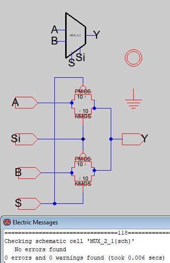
Here
is the schematic of the MUX. Don't forget to put the vdd and the gnd
symbol in the schematic even though it is not used for this specific
schematic. Spice will report errors if vdd and gnd are not there.
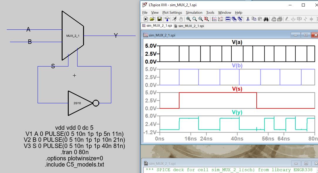
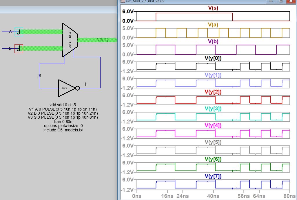
Run the simulation in a new schematic view to verify the logic of the
MUX.
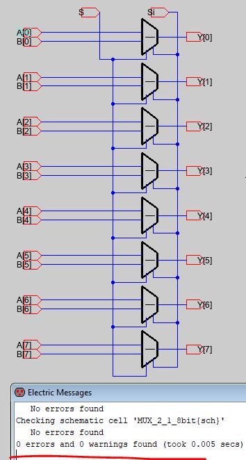
Next let's extend it to an 8-bit MUX. An 8-bit 2-1 bux will select
either of the two 8-bit binary numbers for the output. If we don't use
the buses in electric, the original schematic looks like this (don't do
this, the one uses buses is recommended).
(Again, the following figure only shows you the concept, this schematic
is not recommended. Use the bus version below).
However, let's use the bus to do it in an easier way. All the 'S' and
'Si' bits are being controlled by the same signal so they should be
shorted to 'S' and 'Si' wires not buses.
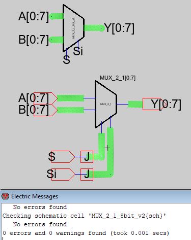
Create a simulation schematic to verify the logic.
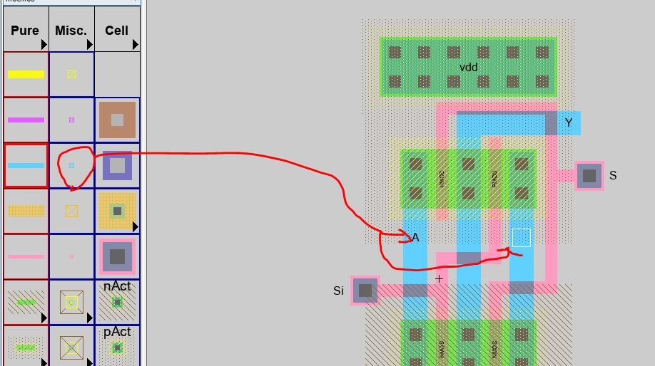
Next, the layout. Let's work on the 1-bit MUX first.
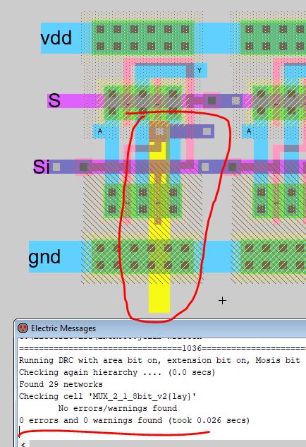
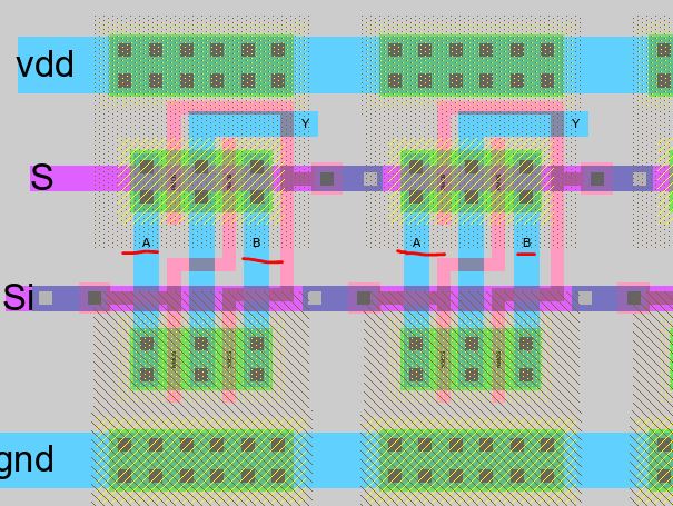
Next, create an 8-bit MUX. There might be very limited space for
routing. If you get wires on Metal 3, you can place the via above the
transistors to gain some spce.
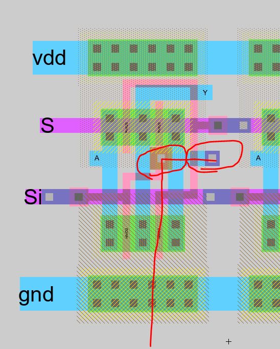
To save more space for A and B, go back to the 1-bit MUX's layout,
place a node directly on the traces and connect the node to the trace.
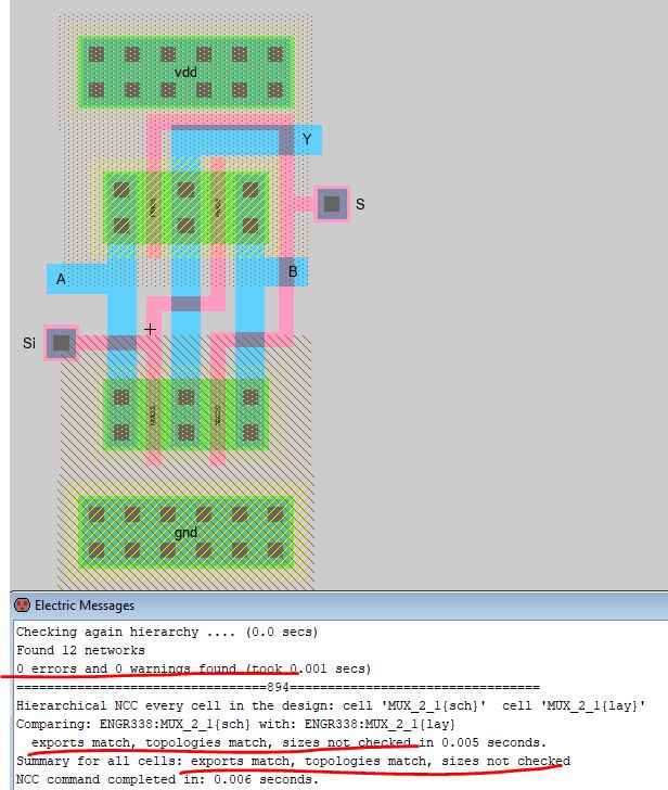
Now, youc an export the node instead of extending the wire out. Don't
forget to run DRC and NCC every time you make any changes to the
subcell.
Next, come back to the 8-bit MUX, you can see that the subcells have
been updated already.
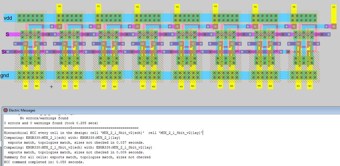
Then finish it up:
Task 2:
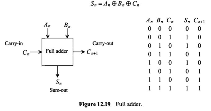
Build a 1-bit high-speed full adder. (40 points)
The
example of this full adder's AOI logic can be found on Page 397-398 on
Dr. Baker's CMOS book.
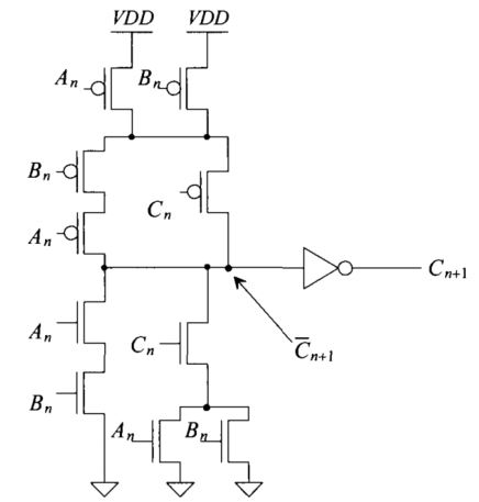
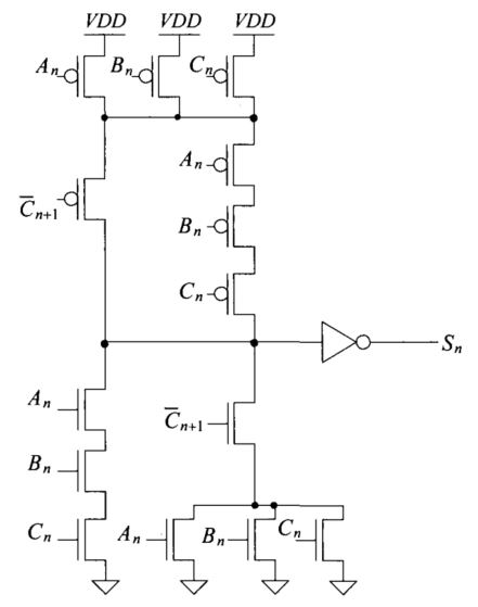
Finish the schematic and the icon.
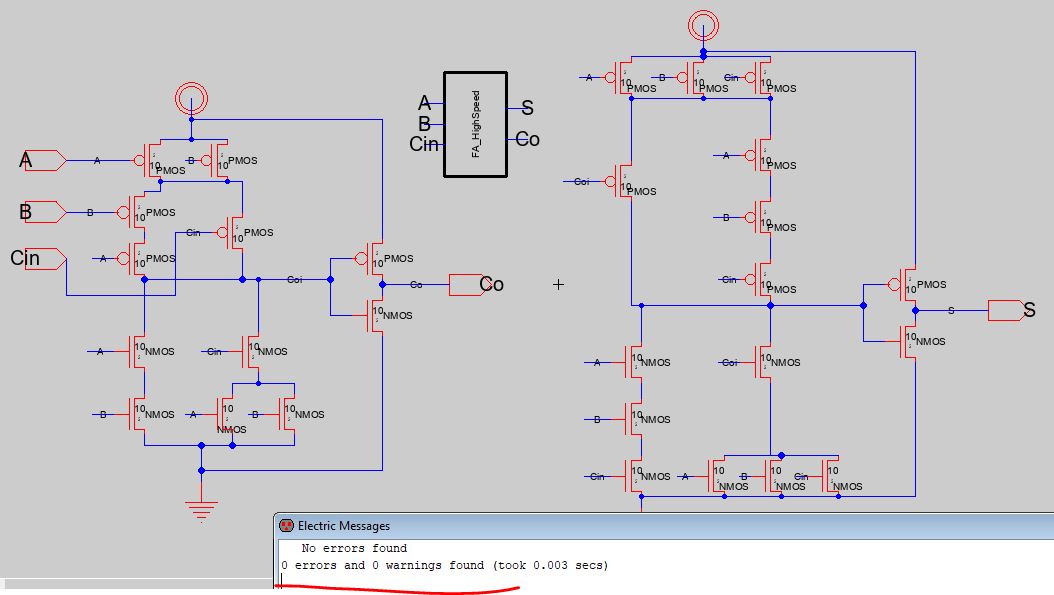
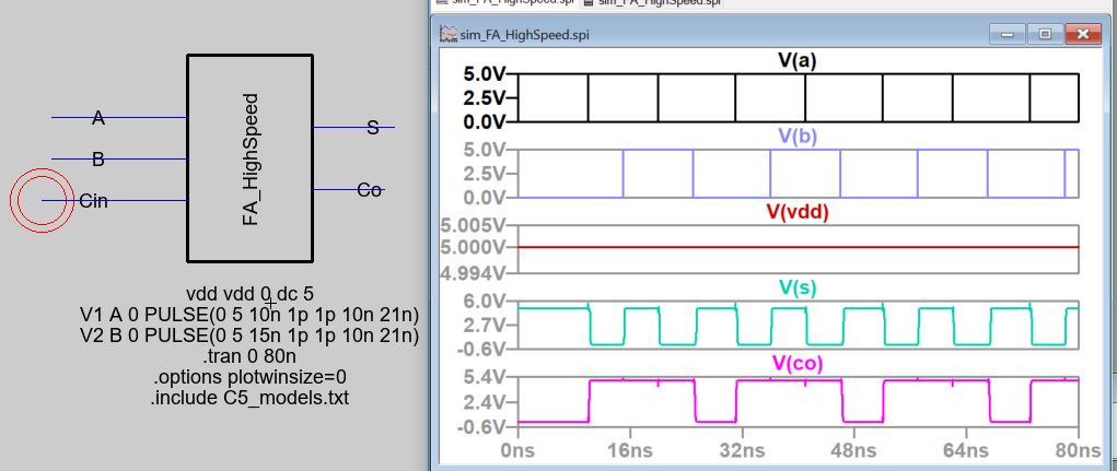
Run a simulation to verify the logic.
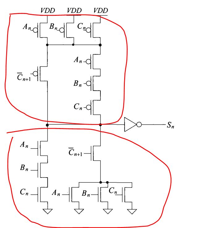
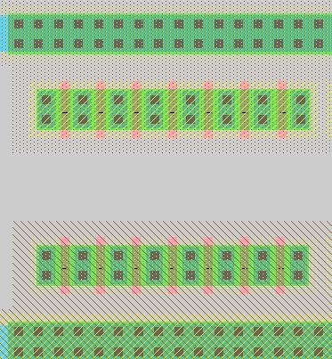
Next, the layout of the high-speed full adder. The trick of organizing
the layout view is to build each part that highlighted in the schematic
first, then make all the gate and drain/source connections.
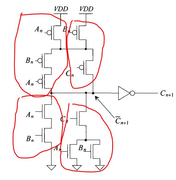
When making the connections, start for each vertical circuit. For
example, the following connections handles the left branch of the
schematic.
Next, move forward to complete all the connections.
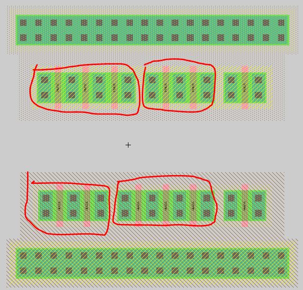
For the second schematic for caculating the summation, I did it more
aggressively. I group all the PMOS and all the NMOS together. In the
layout, I directly put 7 PMOS and 7 NMOS in series in between two
rails.
The two groups:
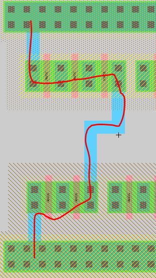
Then, I drew a stick diagram to implement all the connections.
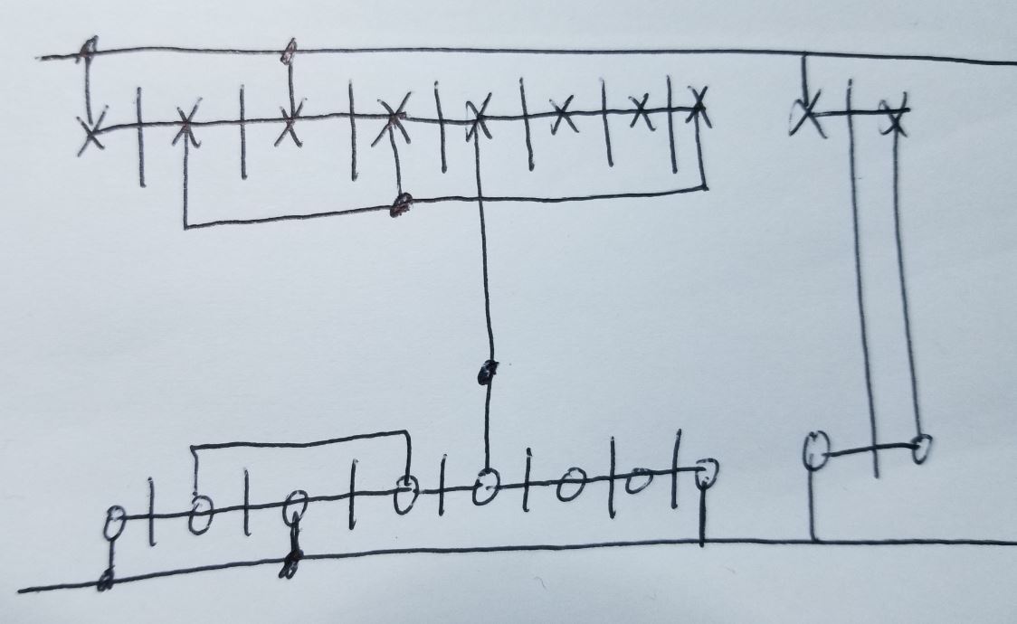
Please note that the MOSFETS in parallel are not in order. Anyone of
the parallel MOSFETS can be A or B or C. The MOSFETs in seies have an
order. The final layout of mine is shown below. This may take you hours
to finish.
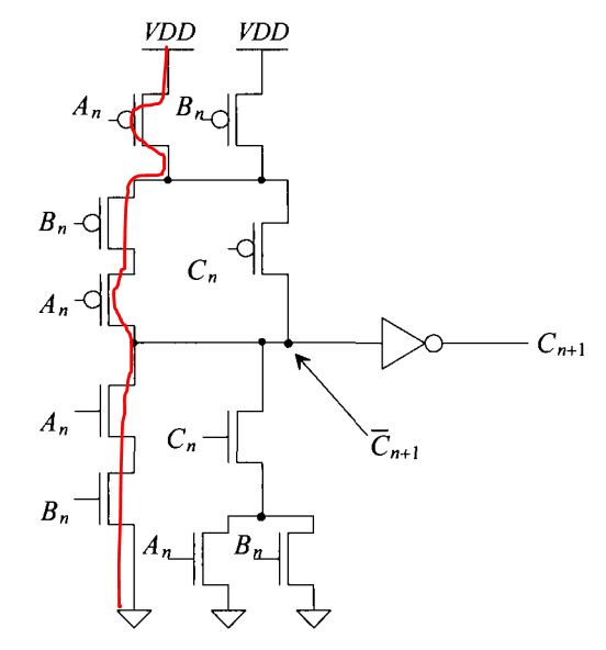
Please note that the left half (for Co) has 4 groups of MOSFETs, 2 for
PMOSes 2 for NMOSes. The right half (for S) has only 2 groups, 1 for
PMOSes 1 for NMOSes. (not include the inverter). You can definitely
have more groups for either side.
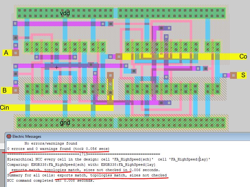
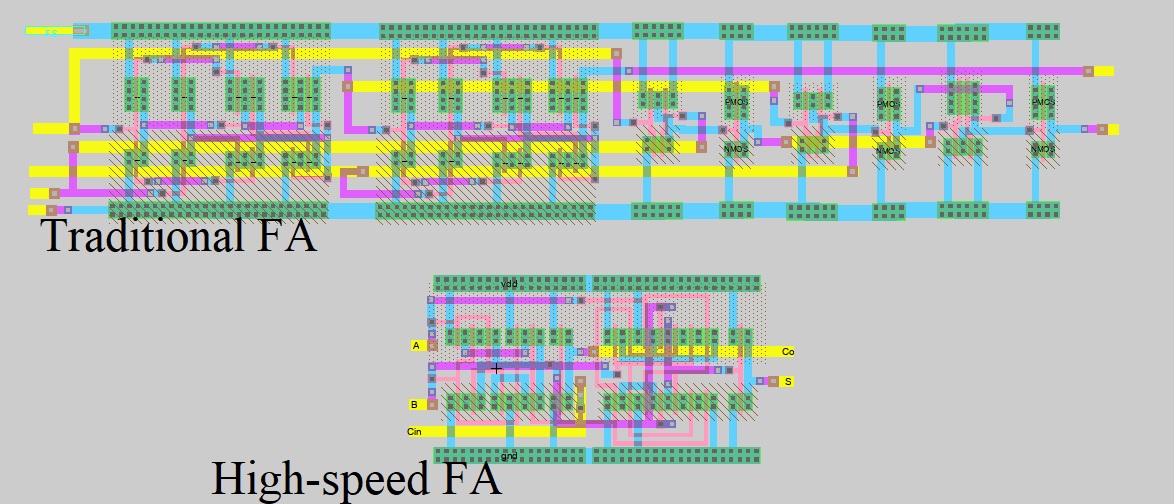
If you copy/paste the traditional FA's layout to the same view, you'll
find that the new one is way smaller than the old one. If it is an
8-bit FA, the saved space will be considerable.
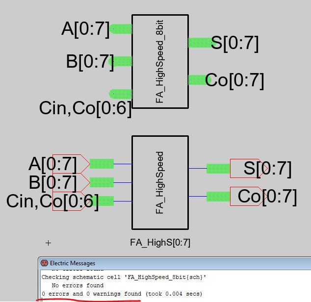
Task 3:
Build an 8-bit high-speed full adder. (30 points)
If your 1 bit full adder works, this step should be travial. I'll not
show the details of it. The main results can be found below.
The schematic:
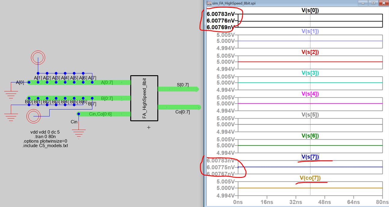
The simulation. Note that A[0] and B[0] are the LSBs. I set two static
8-bit numbers A=11111110, B=10000000, so A+B=S=01111110, Co=1. The
simulation in LTSpice shows the correct answer for it. Run at least 3
simulations in your report to verify the logic of this 8-bit full
adder.
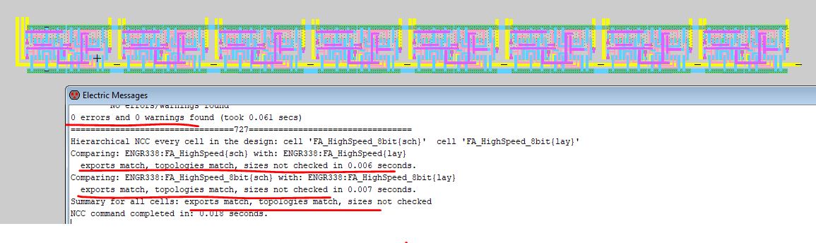
Finally, the layout of the 8-bit full adder.
Lab reports grading rubric:
Task 1: 20 points.
Task 2: 40 points.
Task 3: 30 points.
Writing/formatting: 10 points.
---------------------------------This is
the end of the lab