ENGR338 Digital Electronics Laboratory
Lab 6 Build a NAND, NOR, XOR, and Full Adder (2-week
lab)
Objectives:
1. Build a NAND, NOR, XOR, and Full Adder in ElectricVLSI.
Lab Tasks:
Task 1:
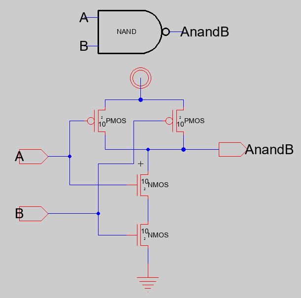
Create the
schematic and layout of the NAND gate. (15 points)
Create a new schematic view for the NAND gate. Design the
schematic, the icon, and the layout of the NAND gate. (The icon must be
in a NAND gate shape, any other shapes are not acceptale).
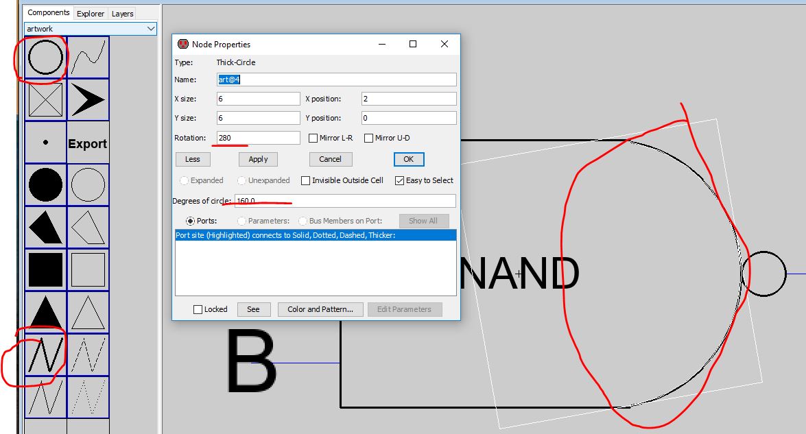
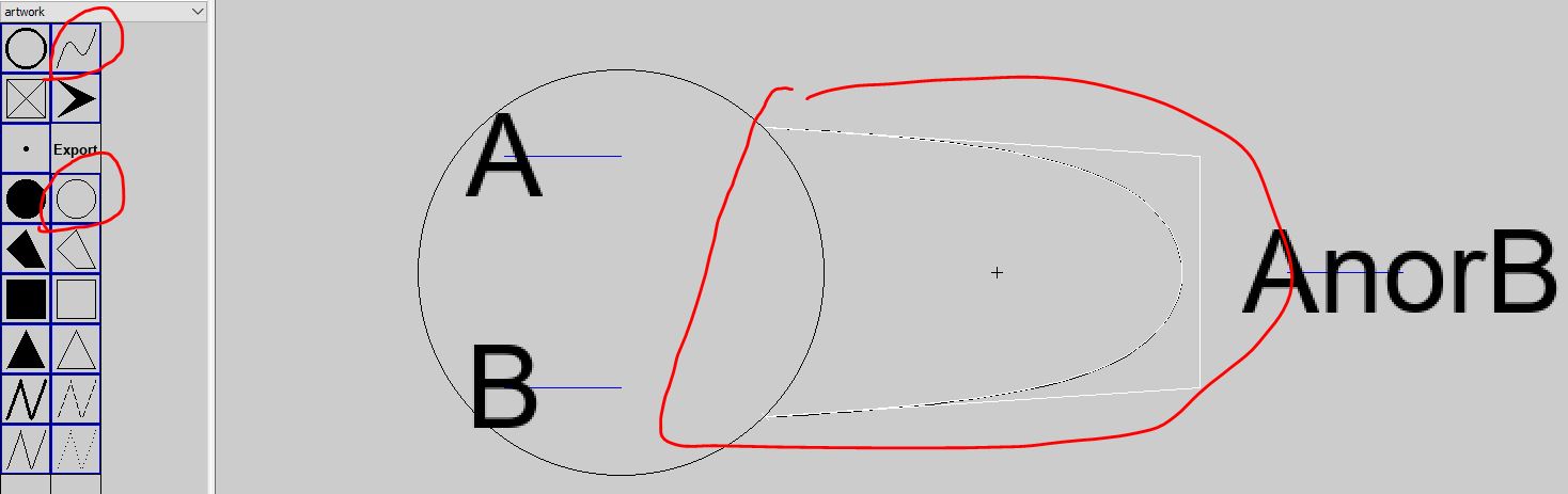
The arc was created from the circle component. The left part of the
NAND gate symbol was created from the polygon tool as indicated in the
folllowing figure. The parameters I used are as follows:
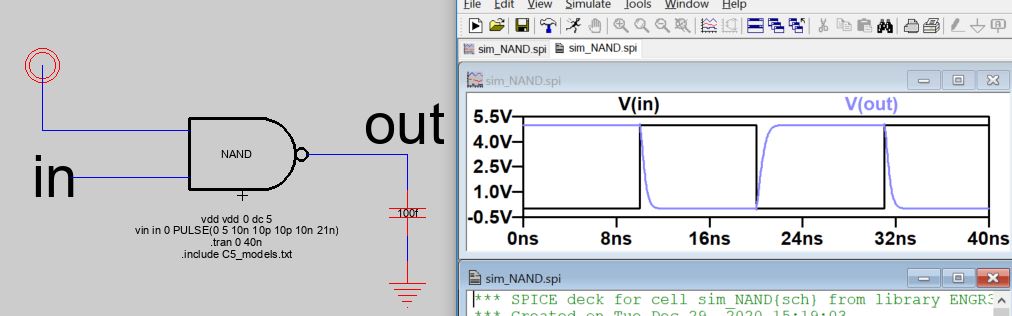
Next, run DRC to the schematic. If it passes, create a new schematic
view called 'sim_NAND' to use the NAND symbol for a simulation.
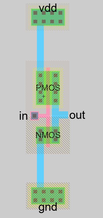
Next, design the layout. The PMOSes are in paralle and the two NMOSes
are in series.
Make the connections.
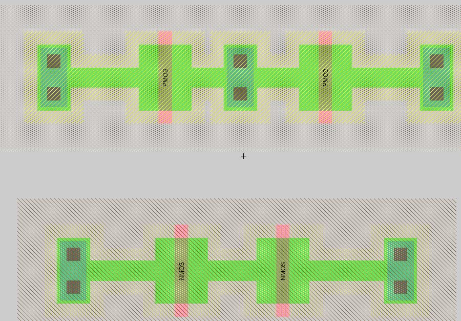
Move them closer to form the MOSFETs. Run DRC before moving forward.
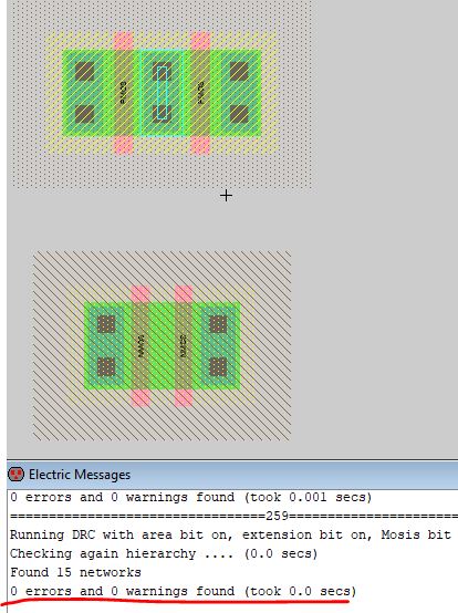
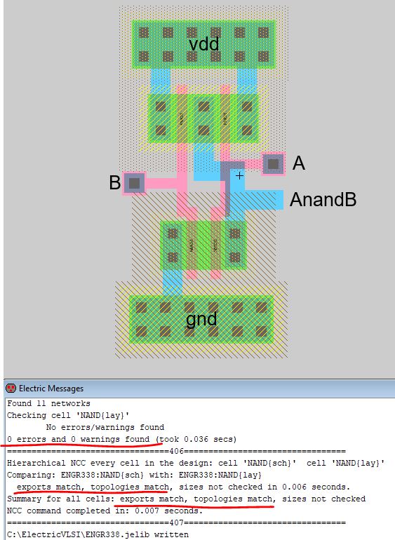
Make the connections and run DRC and NCC (LVS).
Here is a trick. The two PMOSes are in parallel so there is no
left/right order for the PMOSes. However, for NMOSes, the input A is
connected to the NMOS further away from the gnd.
In the layout view, the export A should be connected to the NMOS
further away from the gnd as well. (NCC will report errors if this is
not connected correctly).

Task 2: Create
the
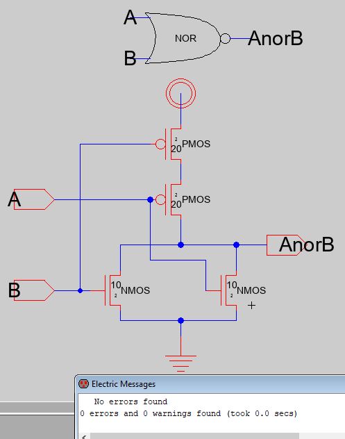
schematic and layout of the NOR gate. (15 points)
Follow
the similar procedure to build the schematic of the NOR gate. The PMOS
was sized as 20/2.
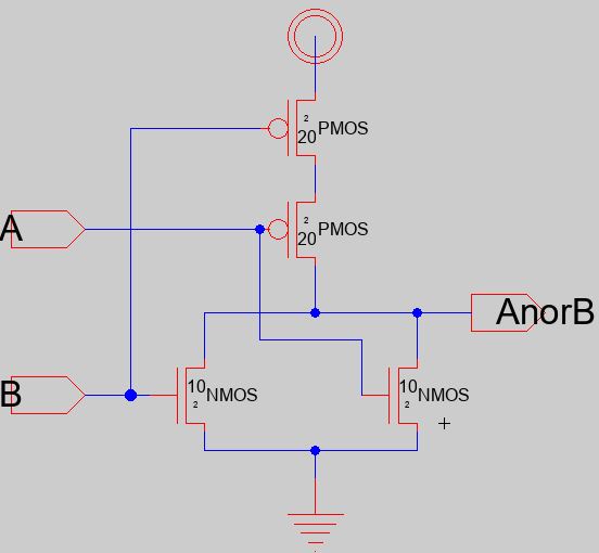
The shape
of the NOR gate's symbol is not easy to draw. The following figure may
help you get it done sooner.
Make sure it is DRC clean.
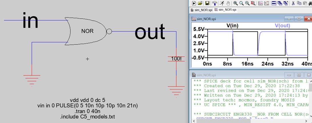
Create a new simulation schematic view to verify the logic before
moving forward.
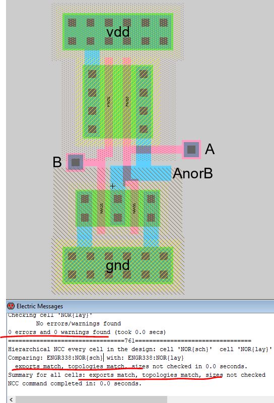
Follow the similar procedure to finish the layout for the NOR gate. Run
DRC and NCC.
Task 3: Design, simulte,
and layout an XOR gate. (30 points)
From Dr. Baker's CMOS book Page 367, we can find the AOI logic for the
XOR gate:
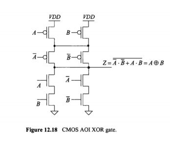
If we don't care about the switching points of the MOSFETS, we can use
20/2 for PMOSes and 10/2 for NMOSes.
The schematic in Electric can be something like the following. Again,
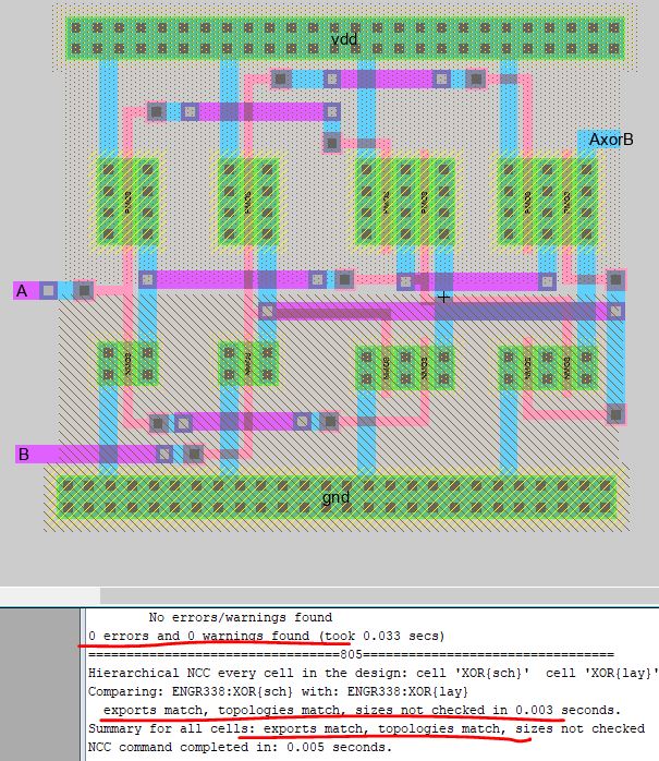
don't move forward if it doesn't pass DRC. (You can use part of the NOR
gate's icon for this one).
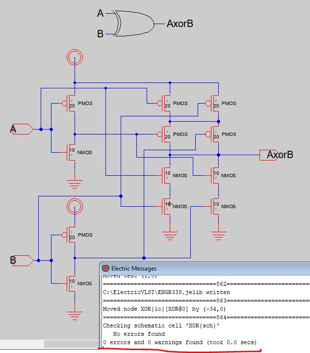
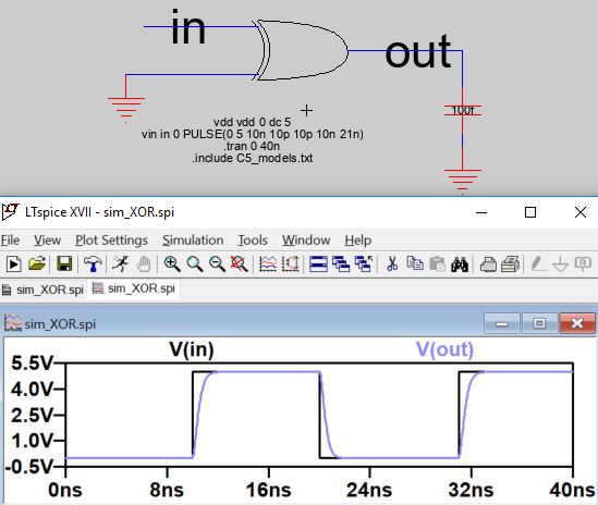
Create a new schematic view and simulate the XOR logic.
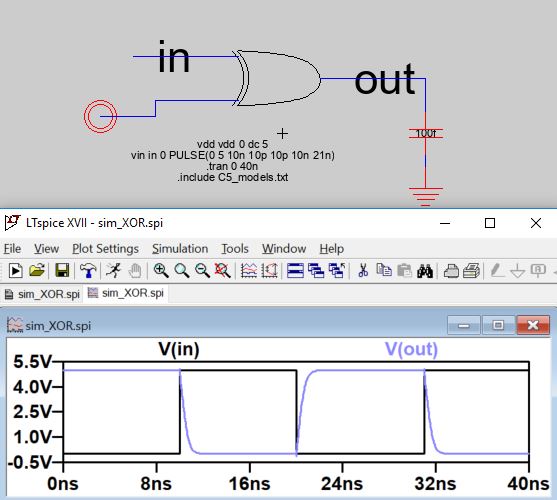
And ground the other input and run it again.
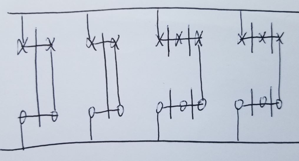
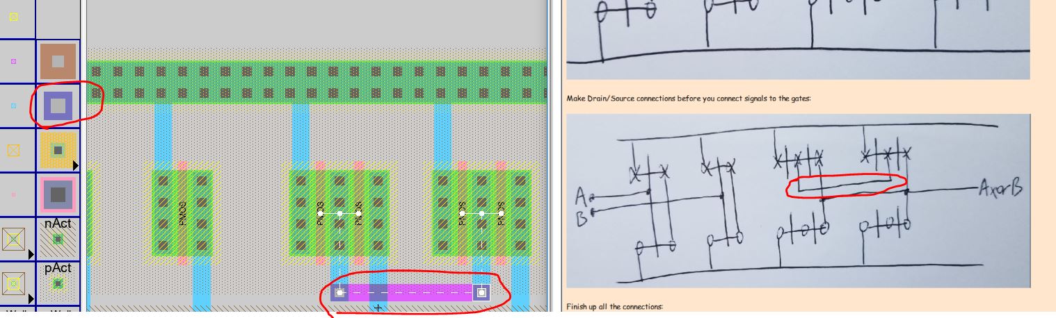
Use the stick diagram to prepare for the layout: ('x' represents PAct,
'o' represents NAct). It'll be helpful if you have different colors of
markers for more complicated circuits.
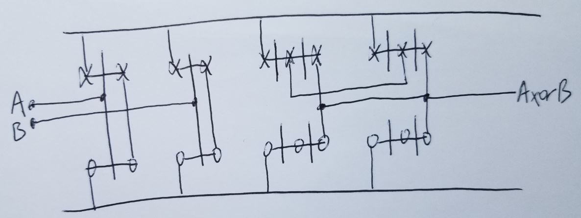
Draw the inverters and other MOSFETS:
Make Drain/Source connections before you connect signals to the gates:
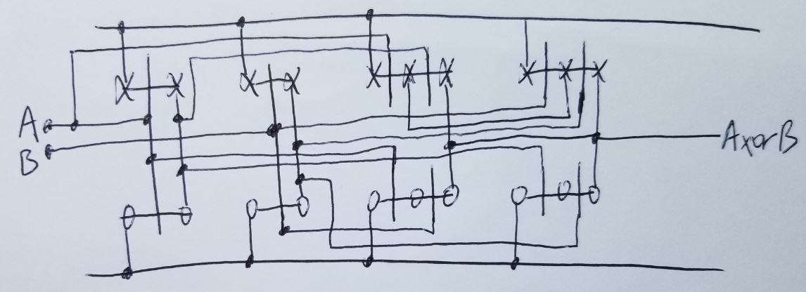
Finish up all the connections:
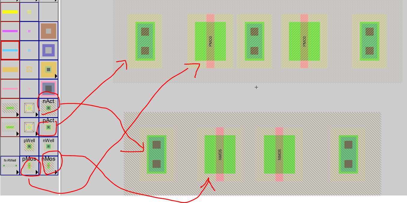
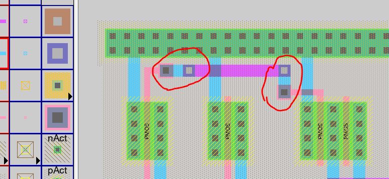
Use pure N-Well-Node and pure P-Well-Node for the PMOS area and the
NMOS area to avoid and DRC well errors. Use the special select button
to select wells.
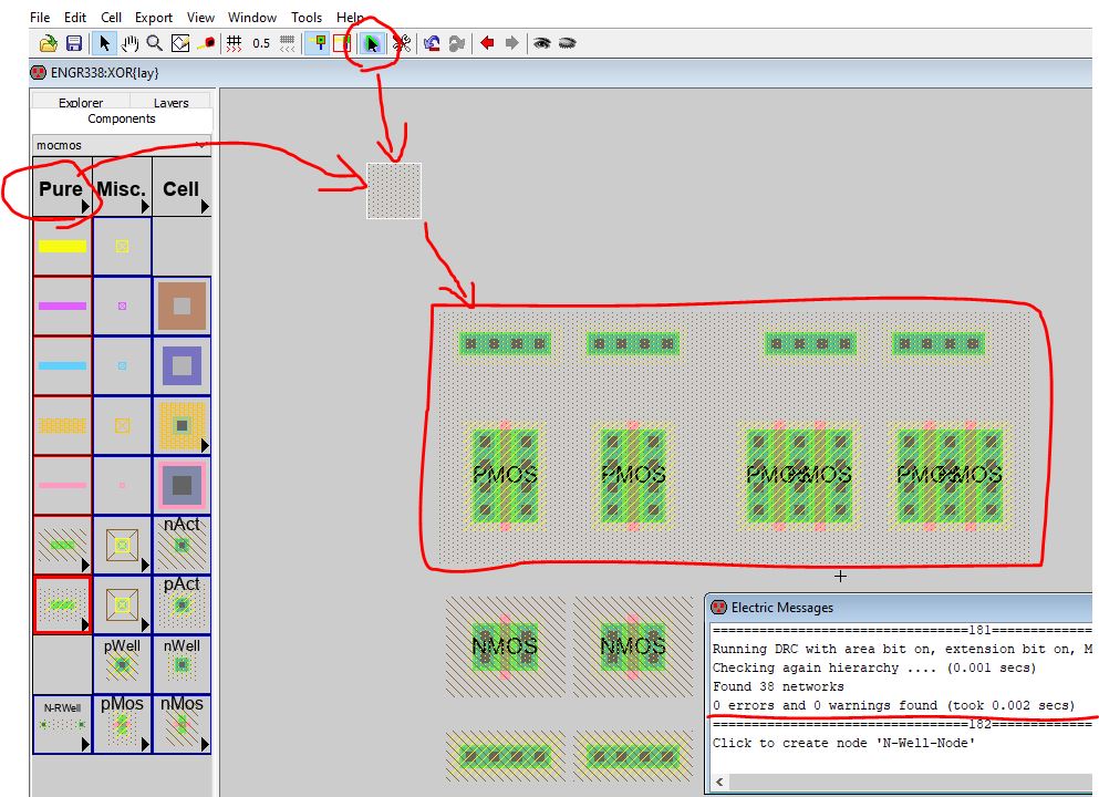
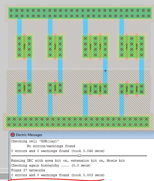
Do it step by step and run DRC checks along the way.
Use the Metal1-Metal2 via to get a metal 2 trace for the following
connection so the circuits are not shorting to each other. Run DRC
check after this step.
Use different metal layers to avoid short circuits. You shouldn't use
long Poly wires which have larger resistance. The gate should be
connected to metal for the routing.
Do it carefully and patiently. Run DRC for every single step. This may
take hours if you are new to Electric. Run DRC and NCC when it is done
for the credit.
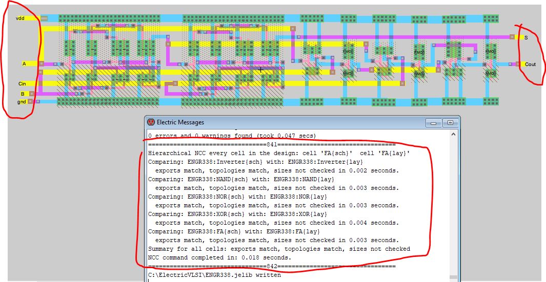
Task 4: Design, simulte, and layout an Full Adder. (30 points)
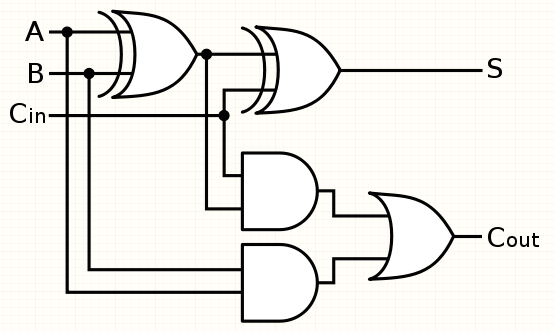
The Full
Adder's schematic can be slightly different. The Full
Adder's logic was derived in one of my CE241's lectures.
Build the schematic and the icon. Run DRC.
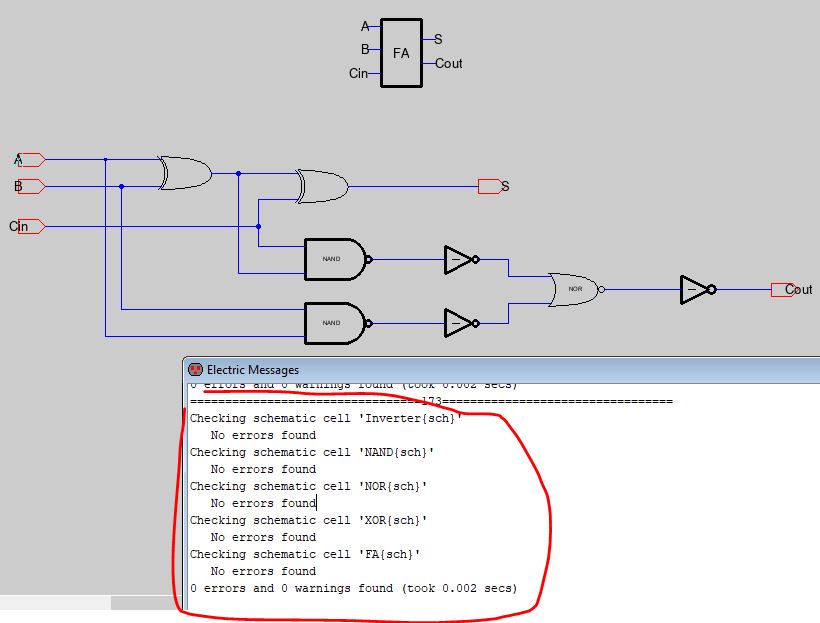
Create a new schematic view 'sim_FA' to simulate it.
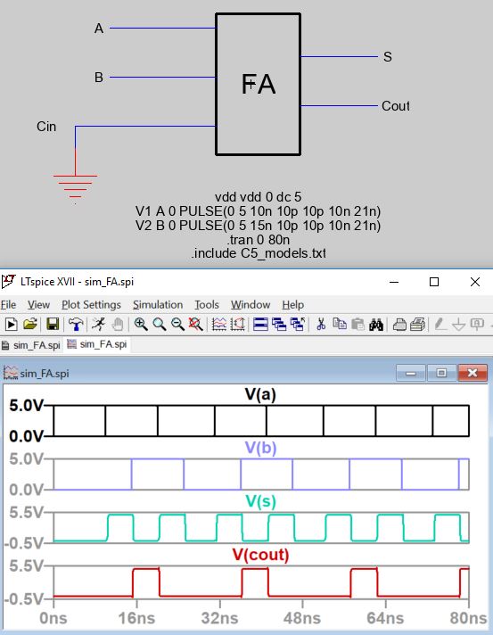
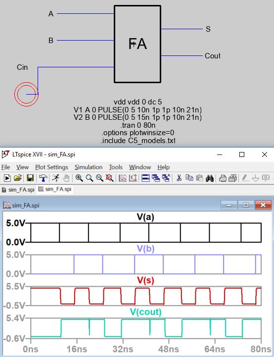
Then connect Cin to vdd to verify the rest of the logic. You can see
that the V(cout) signal has glitches. It is caused by the time delay of
the FA.
Next, build the layout of the Full Adder. This requires a lot of
patience and persistence. It may take hours for you to complete it.
Exports should be on Metal 3.
Before you drag every single gate to this layout view, you should move
the power/gnd rails of each gate to the same height. Use the ruler tool
to measure it before the move. For example, I moved the height to 122
Lambda for all the gates. The following one is the inverter.
The purpose is to place all the gates in a row and they have the same
height.
Lab reports grading rubric:
Task 1: 15 points.
Task 2: 15 points.
Task 3: 30 points.
Task 4: 30 points.
Writing/formatting: 10 points.
---------------------------------This is the end of the lab