ENGR338 Digital Electronics Laboratory
Lab 3 Layout the R-2R DAC
Objectives:
1. Layout the R-2R DAC in Electric VLSI using N-Well resistors.
2. Be familiar with Electric VLSI and LTSpice for integrated circuit
design.
Lab Tasks:
Task 1: Create the
schematic of the subcells for the R-2R ladder. (40 points).
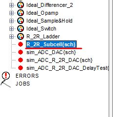
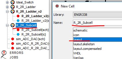
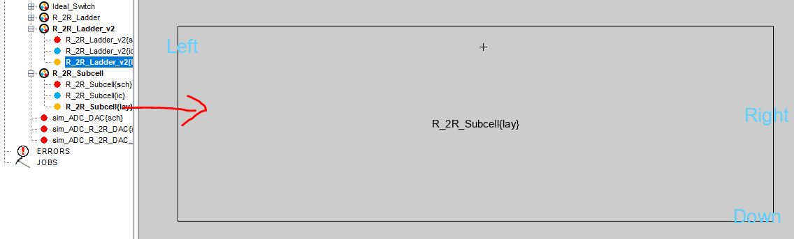
Open your
ENGR338 library in Electric, create a new schematic view called
'R_2R_Subcell'.
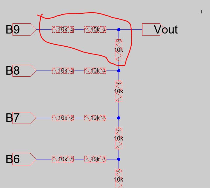
In the R_2R ladder,
there is a repeating structure:
The reason that we prefer using this structure as a subcell is that you
can create a layout of this subcell and copy/paste it to form the R_2R
ladder.
This is a very important trick in VLSI design. You should find the
subcells that repetitively being used in a relatively large cell. After
the subcell is done, perform DRC/LVS check to ensure that the subcell
is working.
Otherwise, it'll be very hard to debug if you laid out a large scale circuit without a
reasonable hierarchy and it reports errors after you are done.
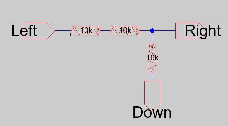
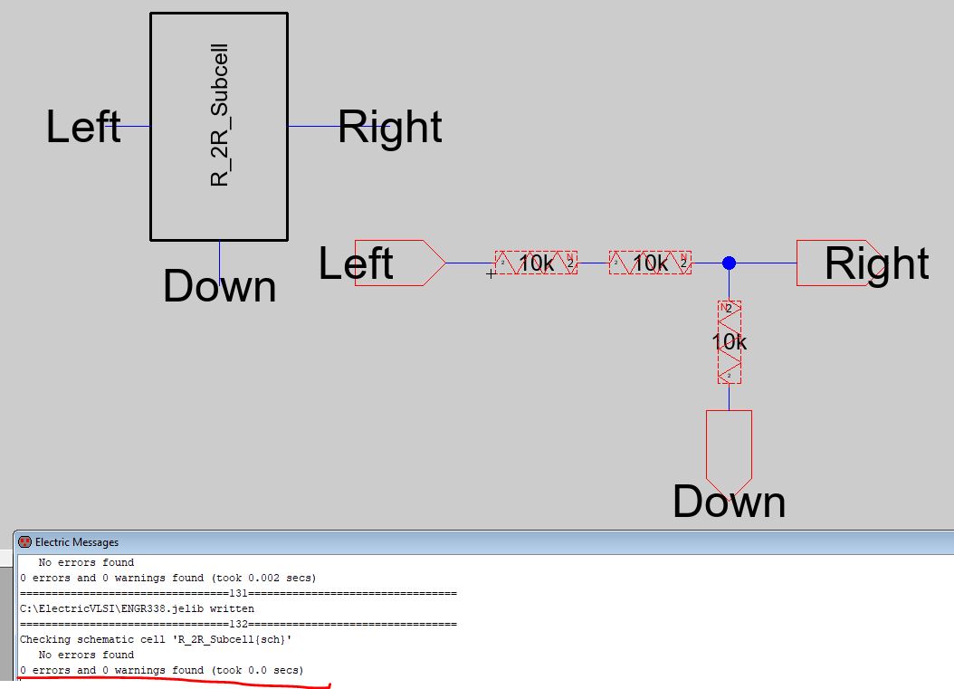
The schematic of the subcell looks as follows:
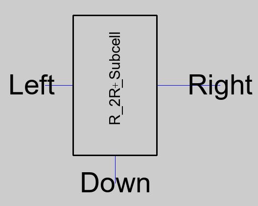
Create an icon view from it:
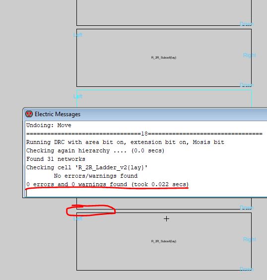
Run DRC: (F5)
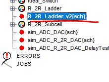
Next, create a new schematic view, call it 'R_2R_Ladder_v2' to
differentiate it from the one in Lab 1.
Drag and drop the subcell icon to this view. Copy and paste 10 of this
in this view. After that, create a icone for this ladder. Don't forget
to add a 10k resistor at the very bottom of this ladder.
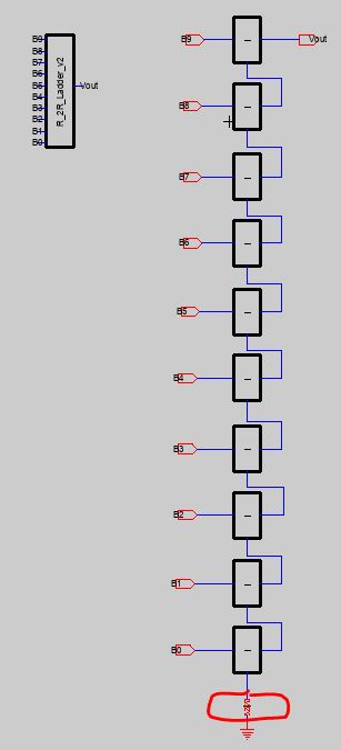
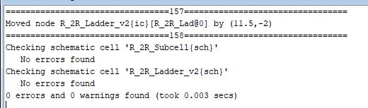
Again, ensure that it is DRC clean.
Task 2: Create the layout of
the subcells for the R-2R ladder. (50 points).
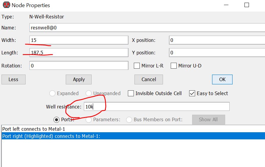
The
sheet resistance of n-well in the C5 process is roughly 800 ohms. The
minimum width of n-well is 12 lambda so let’s make a 10k resistor using
a width of 15 and a length 187.5 (since sheet resistance varies we
could round to 185). Enter the values as seen below.
If
the field for the Well resistance isn’t showing, turn off the software
and open it again. (187.5/15 = 12.5, 12.5 squares x 800
ohm/square = 10k ohm).
We’ll
use these same values when doing the corresponding layout.
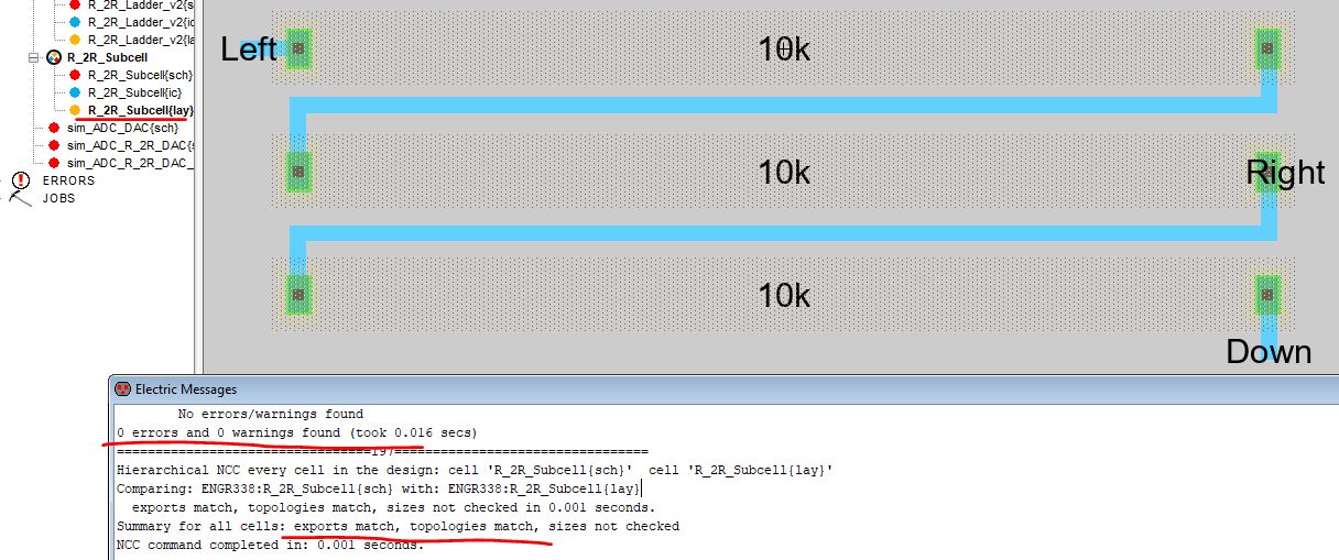
First, create a layout view for the R_2R_Subcell.
Then drag a 'N-RWell' component from the explorer, change the width and
length by pressing 'Ctrl + i'.
Use the coordinator to place the wells at appropriate spots (space them
evenly). I used 25 Lambda for spacing.
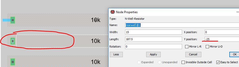
Create the exports at the end of the metals or at the node of the
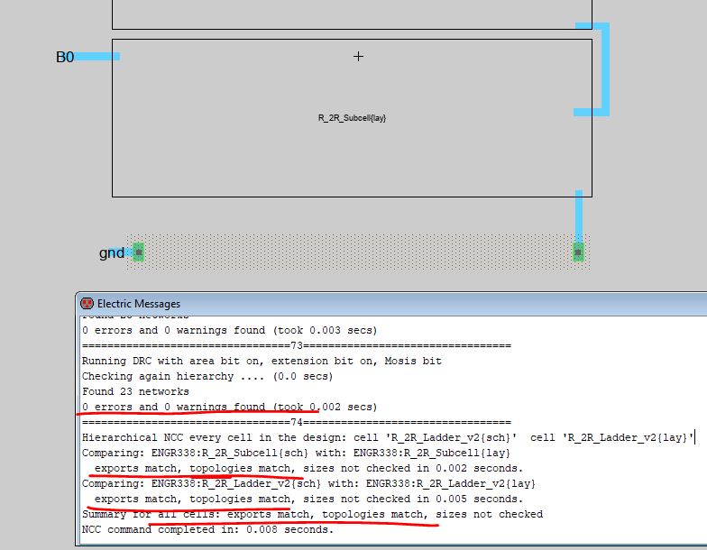
N-Well resistor. Ensure everything passes not only DRC but also NCC (or
LVS).
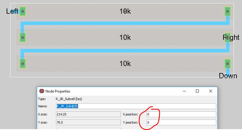
Next, create the layout view for the 'R_2R_Ladder_v2' schematic. Drag
and drop the layout of the 'R_2R_Subcell' to the layout view:
The inside of the layout is hidden and not selectable. This is an
layout icon that you can use to build a larger layout. To make it
visible (still be selectable), click the 'eye button' in the menu.
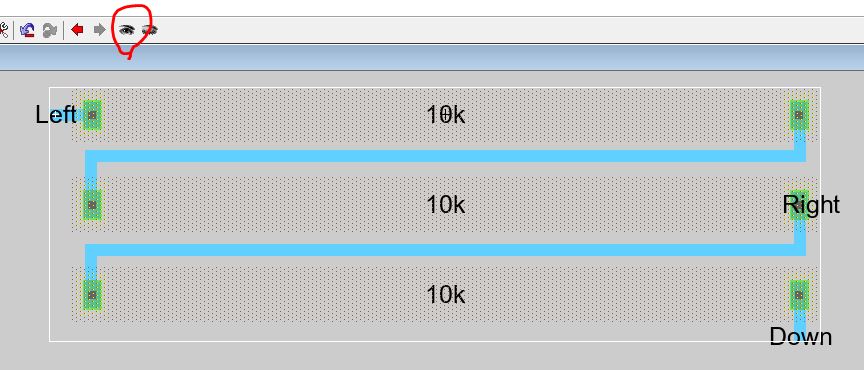
The inside structure is not selectable. The only selectable ones are
the 'off page' ports used to connect to other places in this view.
Before you copy/paste 10 of this cell, place it at the origin (0, 0).
Next, we can use the 'Edit - Array' function to quickly create a
10-cell column out of this.
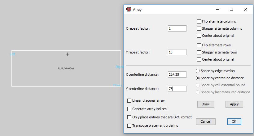
Note, here I used 'Space by centerline distance', and the space is 75
Lambda. If you don't do this, it may not be able to pass DRC since the
wells are too close to each other in the array. Ensure it is DRC clean
before you start wiring everything.
Don't forget to add the single 10k resistor at the very bottom. Ensure
everything passes DRC and NCC.
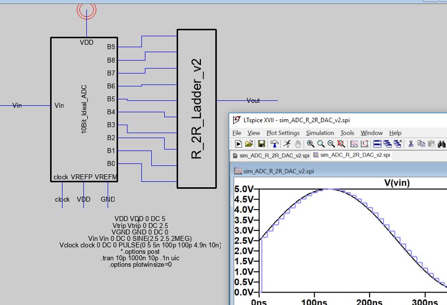
The ADC is ideal so we can't create a
layout of it. Let's just replace the DAC we created in Lab1 in the
simulation and run it. Because this DAC has passed NCC (LVS) with the
layout view, if the schematic works, we can say the layout is correct
too. They have the same netlist and electrical connections which were
verified by NCC (LVS).
Lab report grading rubric:
Task 1: 40 points.
Task 2: 50 points.
Writing/formatting: 10 points.
-------------------------------------
The end of the lab.