Week 4 Data Storage Units
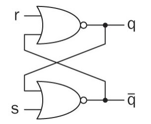
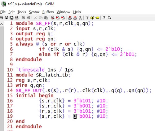
1. SR Latch/Flip-Flop (level triggered)
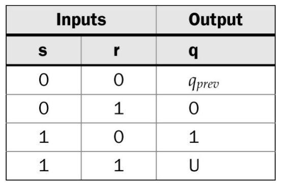
Truth Table
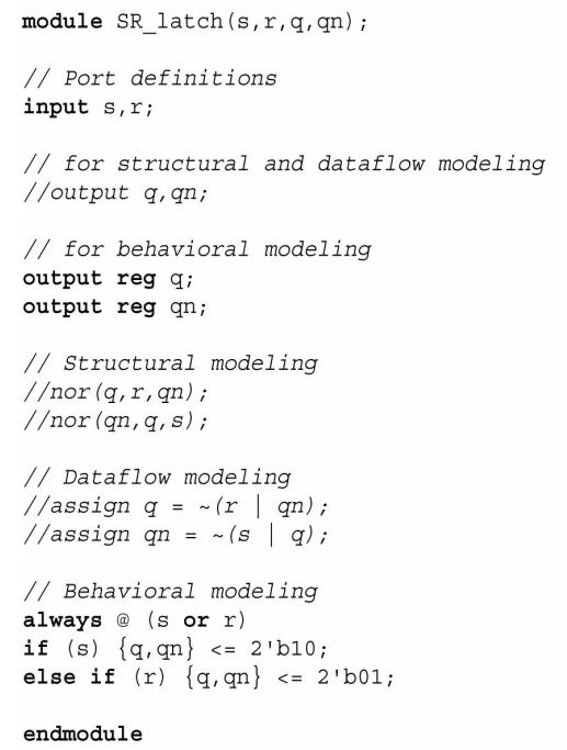
In Verilog:
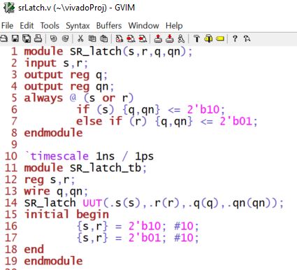
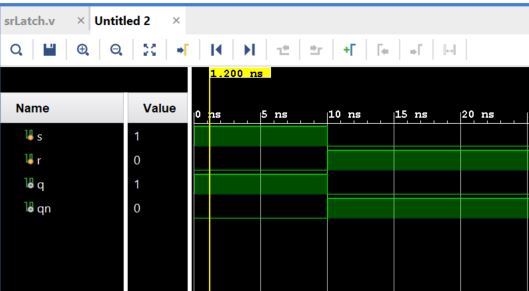
In Vivado:
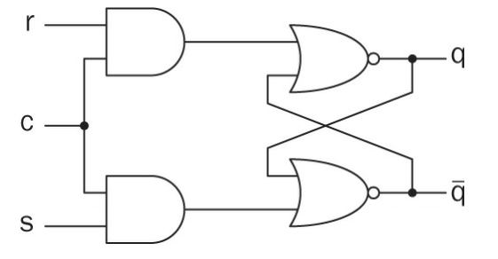
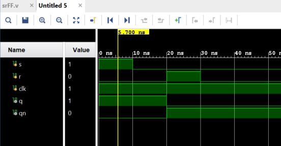
SR flip-flop:
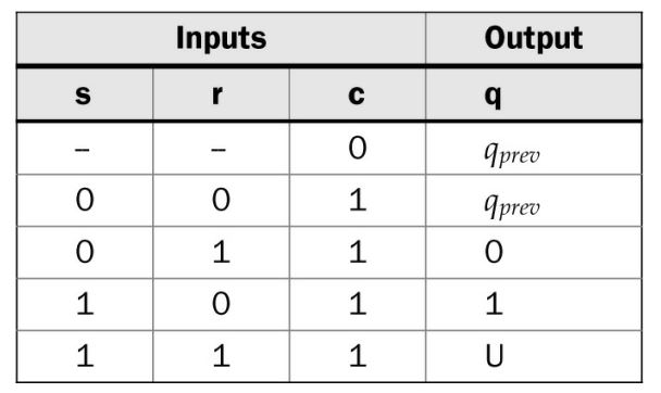
Truth Table
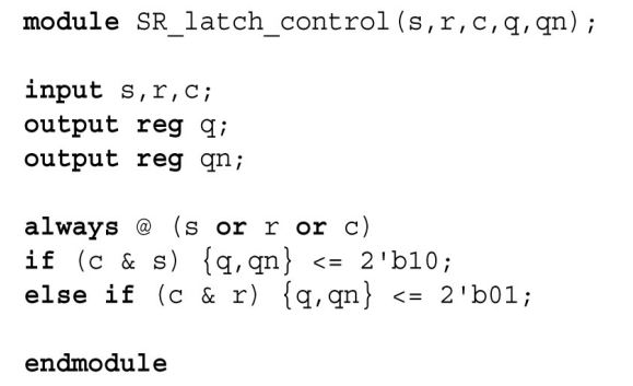
In Verilog:
In Vivado:
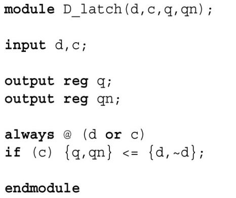
2. D Latch (D Flip Flop, level triggered)
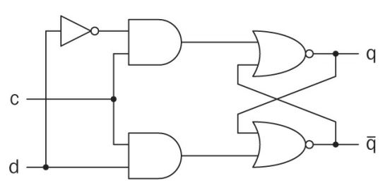
Truth Table
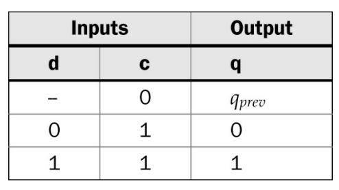
In Verilog:
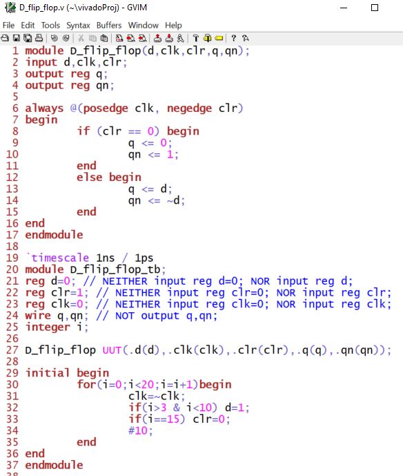
3. Edge triggered D Flip-Flops
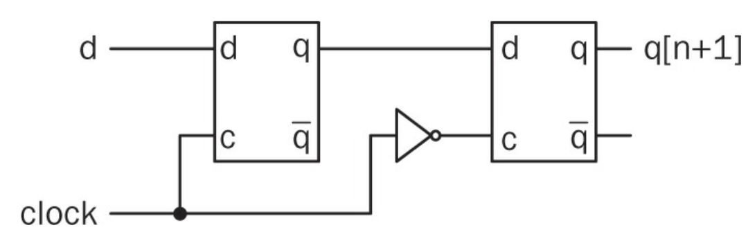
In Verilog:
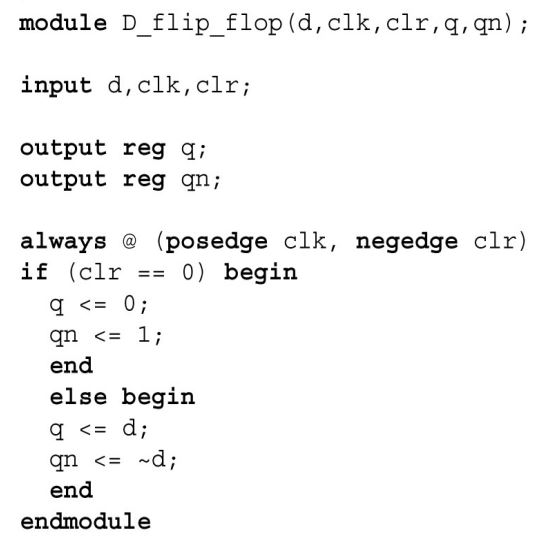
In gvim and Vivado:
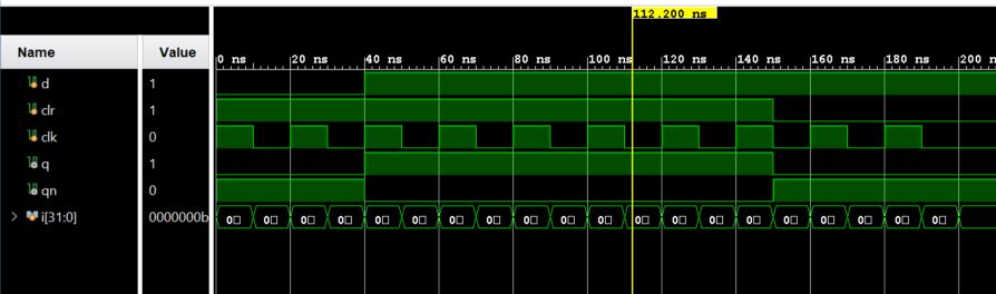
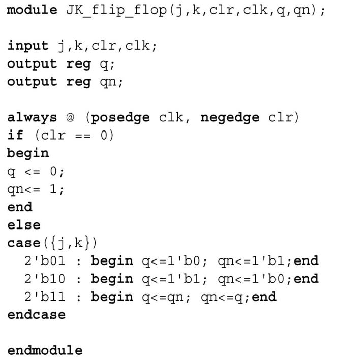
4. Edge triggered JK Flip-Flop
The new device will act similar to the SR latch while eliminating its
undeterminate state. We call this device the JK flip-flop. The circuit
diagram of the JK flip-flop constructed by a D flip-flop is shown
below:
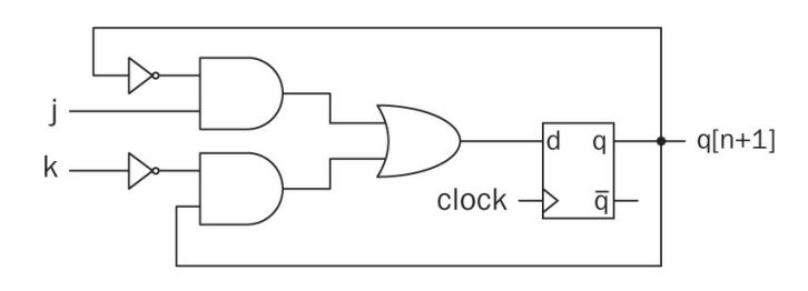
This is definitely not the only circuit desgin of the JK Flip Flop. In
Verilog:
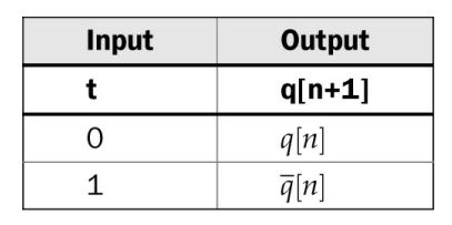
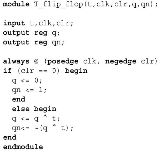
5. The T Flip Flop (Toggle Flip Flop)
We can obtain a specific structure called a T (toggle) flip-flop by
connecting input pins of a JK flip-flop to Logic ONE. Although this new
structure may seem redundant, it will be of great use in counters. The
characteristic table of the T flip-flop is presented in the following
table. As can be seen in this table, the T flip-flop is, in fact, a
limited version of a JK flip-flop such that it either gets input of
logic level 0 or 1. When the input is at logic level 0, the output of
the flip-flop does not change. When the input is at logic level 1, the
output of the flip-flop toggles.
In Verilog: (Behavioral)
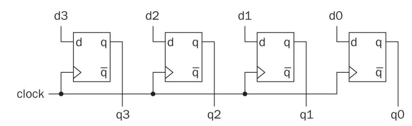
6. Register
A register is an N-bit data storage element constructed by N
flip-flops. In forming a register, flip-flops are connected in parallel
in such a way that data can be processed all at once. We provide the
block diagram of a four-bit register constructed by four D flip-flops:
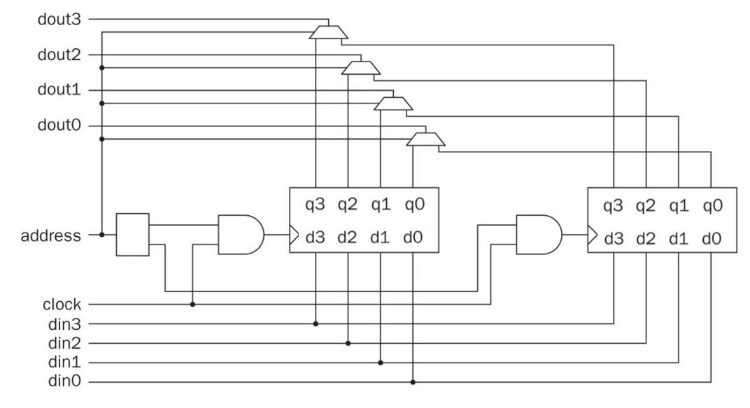
7. Memory
The memory is a data storage element constructed by registers. Within
memory, a specific register should be reached. This is achieved by its
address. More generally, the wires holding the address data are called
address bus. We should be able to write or read the data from a
specific register. The wires used for this operation are called data
bus.
As can be seen in this figure, the data input to two separate registers
are done in parallel. An input register is selected by a one-to-two
encoder in such a way that the selected register gets the clock signal.
The other register not receive the clock. Hence, it will be disabled.
The data output from registers are selected by multiplexers. Both data
input and output locations are selected by the address bit. Although
this is a simple setup, it shows how the memory works.
8. ROM (Read Only Memory)
The stored data may be taken as static during operation of a digital
system. In other words, the data in a specific memory location should
not be altered within the system. Such a location is called read-only
memory (ROM).
The ROM content can be loaded either in a binary or a hexadecimal form.
To use the binary form, the command $readmemb should be used.
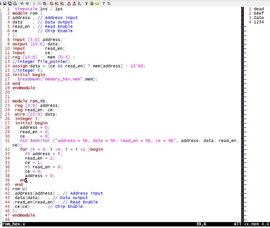
Construct a rom memory in verilog:
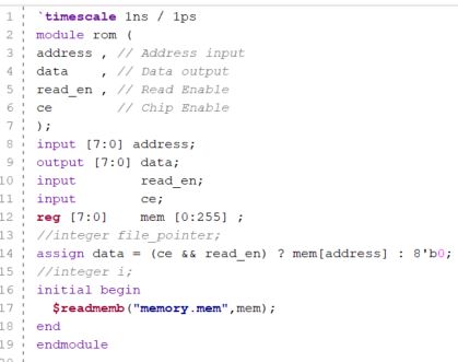
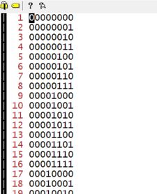
The 'memory.mem' file has 8-bit binary numbers which are separated by
new lines. Use '$readmemb' to read binary files and use '$readmemh' to
read hex files.
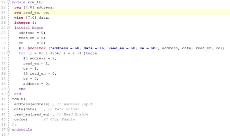
The testbench can be writen directly below the rom.v in the same
window/file, so it becomes: (the 8-bit address has a 2^8=256 depth in
the memory).
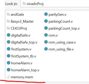
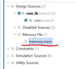
Before run the simulation, don't forget to add the memory file
'memory.mem' as a design source. Only the '.mem' extension worked.
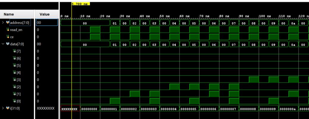
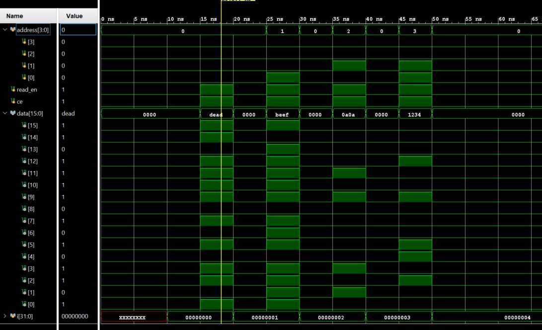
The simulation results in Vivado:
Now, let's modify the memory file to store 4 hex data there and load it
in the testbench. Here is the functioning code for it and please
identify the changes I have made compare to the previous one.
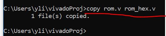
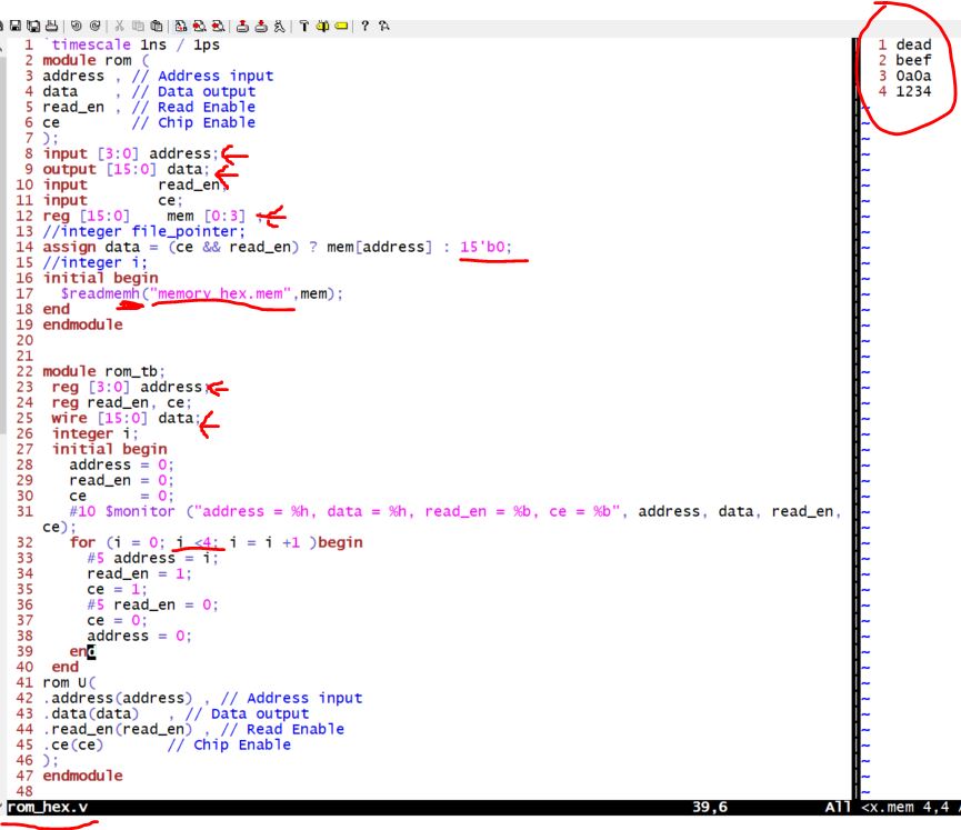
In the command window, duplicate the rom.v and memory.mem files and rename them as rom_hex.v and memory_hex.v respectively.
Open one file first using 'gvim rom_hex.v' in command line, and then in
the opened gvim window, do ':vsp memory_hex.v' to open the other one
aside. Make changes to them. Using 'ctrl ww' to switch between windows.
Please note that the 4-bit address in the following script is
unnecessary. For a memory depth of 4, you only need 2 bits for the
address.
After the changes are made, reload them to the vivado interface and
save them. Run the simulation to show the following results.
Results:
These are the changes I have made to the files.
The memory_hex.mem or memory.mem consists of text hex/binary values
separated by whitespace: space, tab, and newline all work. You can mix
the whitespace types in one file. Comments are the same as regular
Verilog files: // begins a comment. The data width in the .mem file and the verilog file must match.
The following data file has new lines as the separator: (they are hex number)
dead
beef
0a0a
1234
Please
note that the 4-bit address in the following script is unnecessary. For
a memory depth of 4, you only need 2 bits for the address.
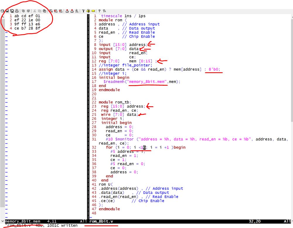
The following memory file has space and new lines as the separator.
There is no difference between space and a new line to separate the
data so the data width is 8 binary bits or bytes. Use the
same method to create the 'memory_8bit.mem' file and the 'rom_8bit.v'
file and make the following changes to them.
Please
note that the 16-bit address in the following script is unnecessary. For
a memory depth of 16, you only need 4 bits for the address.
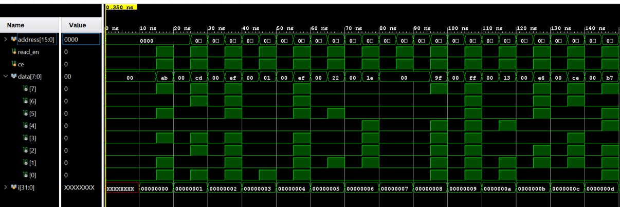
Run the simulation and you should see the follwing results.
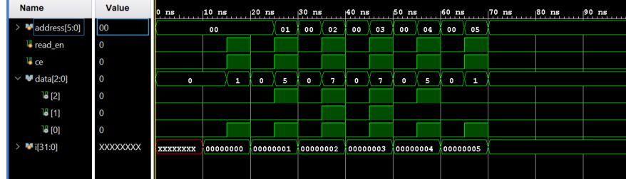
Next, let's use 3-bit binary numbers as data in the memory file.
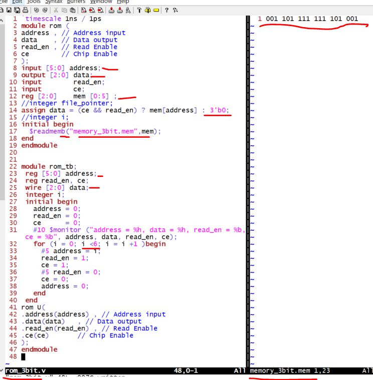
The simulation results:
Next, let's see how to use Vivado IP blocks:
Add a IP core. Double click the area indicated by the red circle.
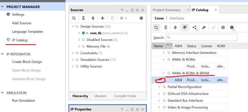
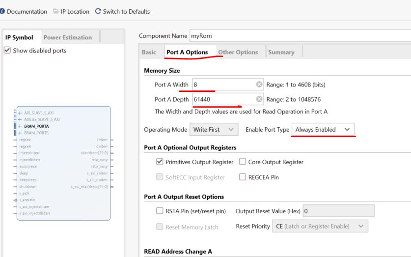
The following window will pop up. Give it a name and select 'single port ROM'.
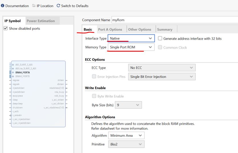
If you click the '+' sign you can expand the ports and you will see the ports 'addra[15:0]', 'clka', and 'douta[7:0]'.
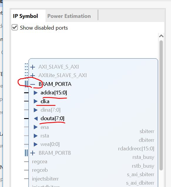
The clka port indicate that there is a clock pin that send the address
to it at the rising edge. The 8-bit digital out only updates at the
rising edge.
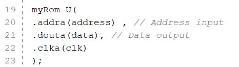
In the testbench, you can instantiate the Rom as follows:
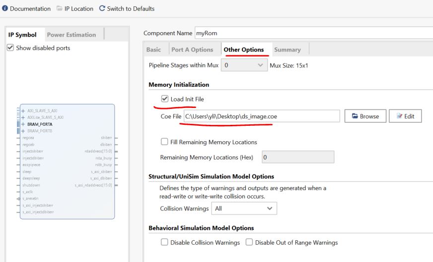
Write the testbench to extract data from the ROM IP core. The ROM stores the data from this file.
Please keep in mind that there is a limit number of 'for loops' you can
run in Verilog. Within the limit, you should demonstrate that the ROM
data is being extracted.
-----------------------
Tasks
1. Repeat the simulation in Sections 1 - 3. (20 points)
2. Write the testbenches and run simulations for Section 4 and Section 5. (20 points)
3. Repeat all the work in Section 8 and complete the task described in the end of Section 8. (60 points)
-----------------
References:
[1] http://asic.co.in/Index_files/verilogexamples.htm
[2] https://web.mit.edu/6.111/volume2/www/f2019/handouts/labs/lab3_19/rom_vivado.html