ESP32, MPU6050 Interfaces and the PCB Design - Part 2
1. Power supply
1.1 Identify the appropriate low-dropout (LDO) voltage regulator
The dropout voltage is the
difference between the output voltage and the input voltage at which
the circuit quits regulation with further reductions in input voltage.
In this project, we are going to use a 3.7 V Lipo rechargeable battery
to power up a 3.3 V wearable device. Wearable means it has to be small
in size and power efficient.
From the schematic of the ESP32 module, it seems like the ESP module only needs VCC, GND, and a ripple-removing 100 uF capacitor to operate. The ESP normally draws 130 mA (https://techexplorations.com/guides/esp32/begin/power/)
when it is powered up by 5 V from USB. We are using a 3.7 Lipo battery
instead of 5 V so the current draw can be a little bit higher than
this.
Compare to the ESP module (wireless modules consumes more power), the
MPU6050 module's power consumption is negligible (below 10 mA).
Therefore, the entire power consumption when the system operates in
wireless mode will be within the 200 mA range.
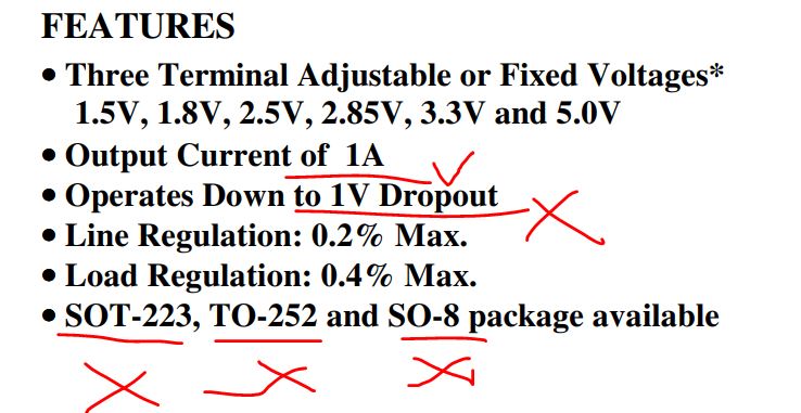
Now it's time to identify the appropriate voltage regulator for our
board. We have been using AMS1117 3.3V, now let's take a look at it's
datasheet to see if it will fit here:
Output current is 1A, which is a lot higher than the 200 mA required for the system, so this feature is good.
1V Dropout???? Goodness, if our Lipo battery provides 3.7V, and we
expect 3.3V output, but AMS1117 will only give us 2.7V output? Alright,
AMS1117 is not a good fit.
Look at the package options: SOT-223, TO-252, SO-8 of AMS 1117. All the
three pakcage options are too big for the system. We need a small
footprint, like SOT-23-5.
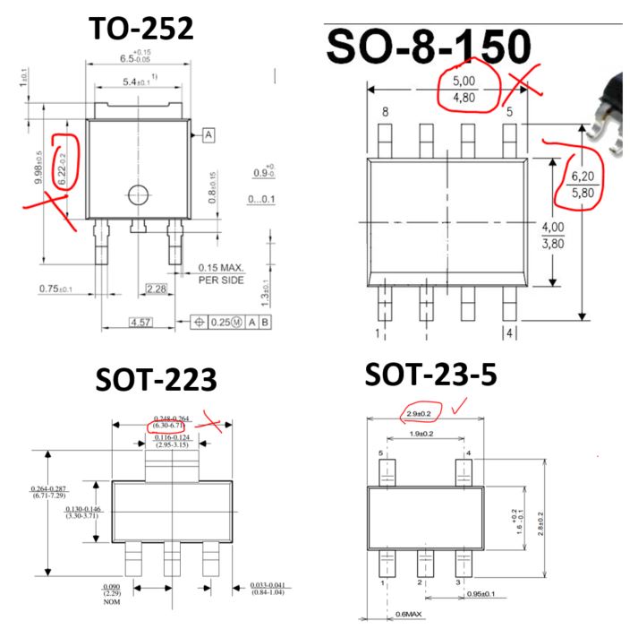
Compare the footprint of SOT-23-5 to SOT-223. SOT-23-5 will save you a lot of space on the wearable device.
So
now what we need is a voltage regulator that provides 3.3 V from a
3.7 V Lipo battery, in the SOT-23-5 package or similar, and the output
current cannot be less than 150 mA in theory. In real life, I'd suggest
pick up a regulator that has the maximum output somewhere around 300 mA
or higher).
From AMS, the company's website, I found AMS 3106 and AMS 500 will fit:
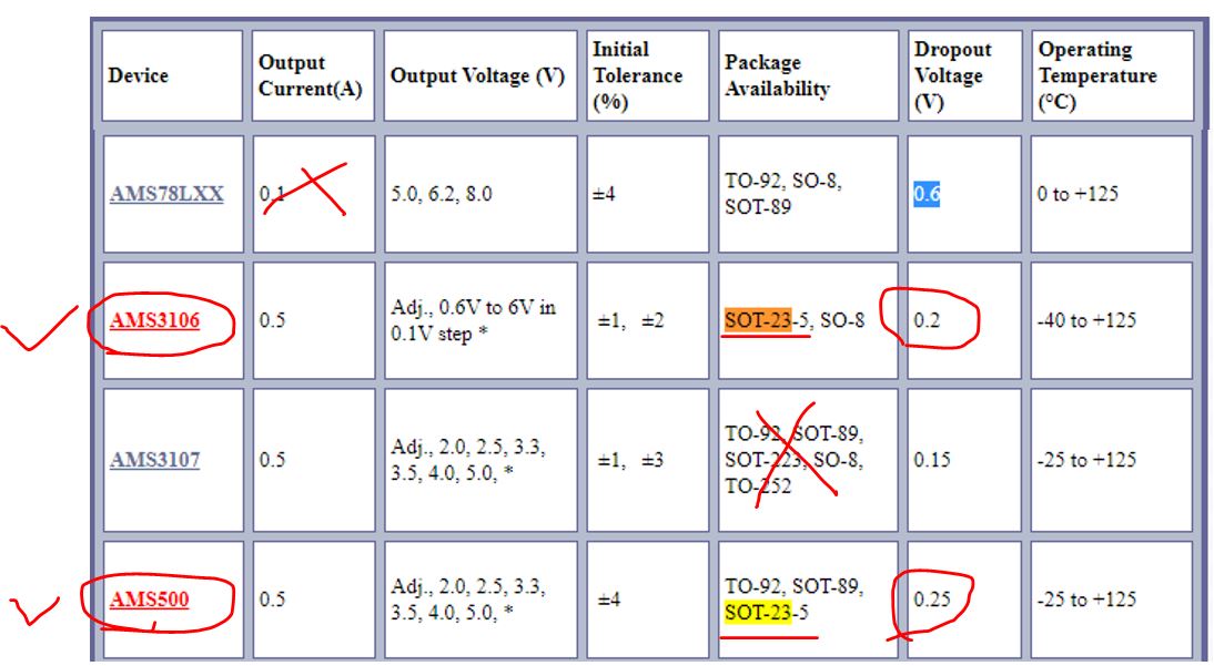
I was not able to find either of these two chips in DigiKey or anywhere else.
Let's see if TI (Texas Instrument) has good ones.
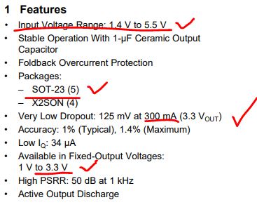
I found an alternative one - TLV743P (datasheet), maximum output 300 mA, Low-Dropout Regulator (LDO):
300 mA is a little bit of concern.
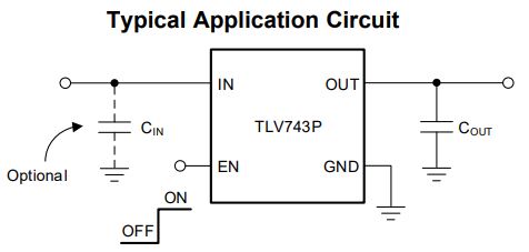
The typical circuit:
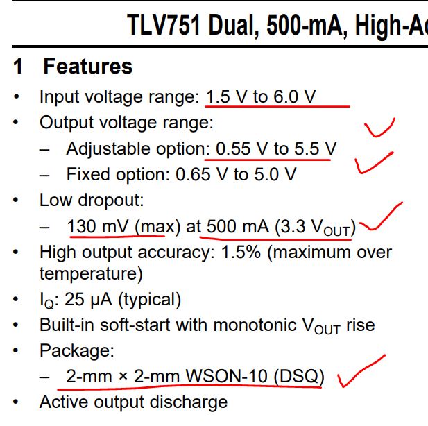
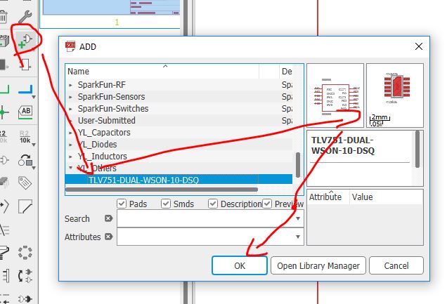
Here is another one: TLV751 (datasheet), and the SOT-23-5 version TLV758P (datasheet).
The typical circuit:
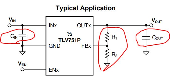
If you conpare these two
LDOs, TLV751 has 500 mA and a smaller footprint (2mm x 2mm), TLV has
300 mA and a slightly larger footprint (3mm x 3mm). However, TLV751
requires two more resistors than TLV743, and resistors take space on
the board. Overall, the cost of space for TLV751 and TLV743 on the
board are similar.
I am more comfortable with the 500 mA TLV751.
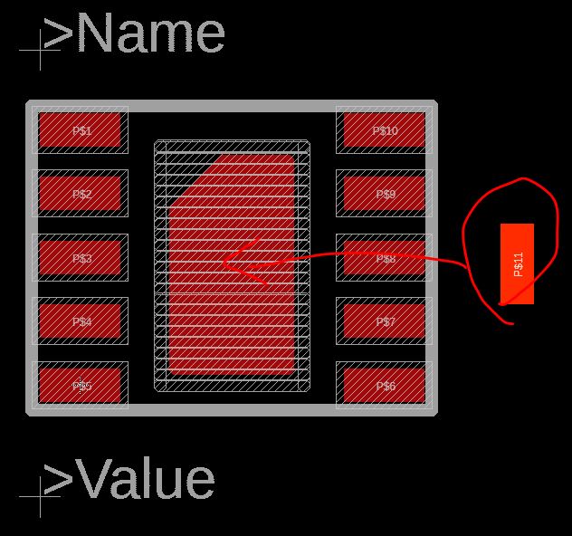
The 2mm x 2mm WSON-10 (DSQ)
package has all the pads at the bottom of the chip so it can be a
little more difficult to solder, but I think I can handle that.
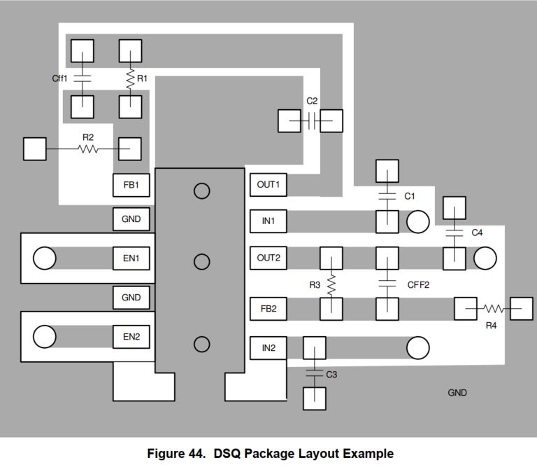
The recommended layout example from the datasheet:
1.2 Design the schematic/layout of the DC power supply
The typical schematic is provided in the datasheet.
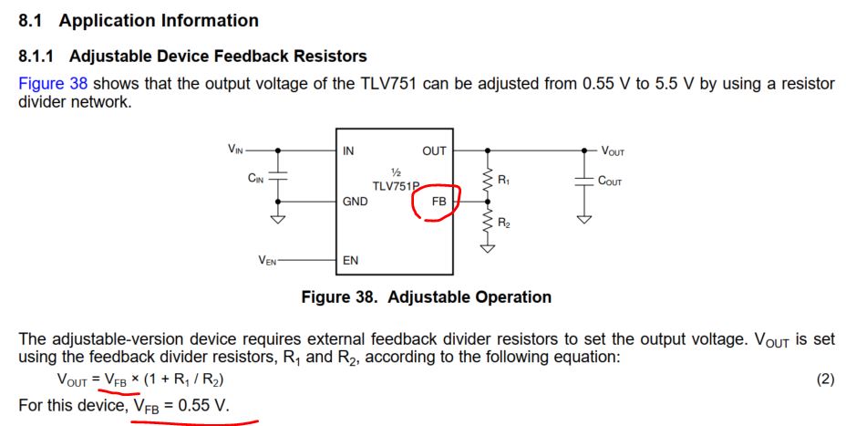
The equation to calculate Vout is very obvious, which is just a simple
voltage divider. VFB is given, which is 0.55 V, you can pick up the
correct resistor pair to form a 3.3 V output. 3.3 = 0.55 x (1+R1/R2),
so R1/R2 = 5.
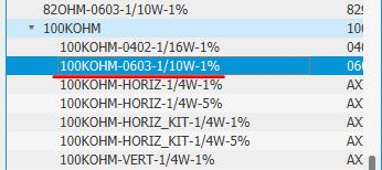
I'll pick up R1=100 k and R2=20 k, and always, pick up the 0603
footprint for the design, which is small but not too small to be
handled by your tweezzer and your iron.
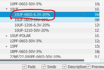
Also, we will pick choose Cin=10 uF, Cout = 10 uF. Cin and Cout are
used to smooth out the ripples of the input/output voltages. Same 0603
footprint for the capacitors.
From the ESP32-WROOM's schematic, the power module looks like this:
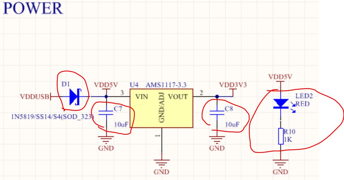
D1 is the Schottky diode used for preventing kick-back voltages and
also used for smoothing out the input voltage while working with the
capacitor. Let's take a look if we should use it.
For example, the S4 (SOD_323 footprint) one. The footprint is pretty small:
However, the forward voltage is somewhere around 500 mV! which means we
are expecting a 0.5 V loss if we use it. The Lipo battery we are going
to use is only 3.7 V if it is fully charged. Why not use a 2-cell
version to get you 7.4 V? It's too big for the our wearable device!
Let's forget about the Schottky device. The voltage supply is directly
from the battery, we we don't actually need it if we never power it up
using an AC-DC adaptor plugged into the wall.
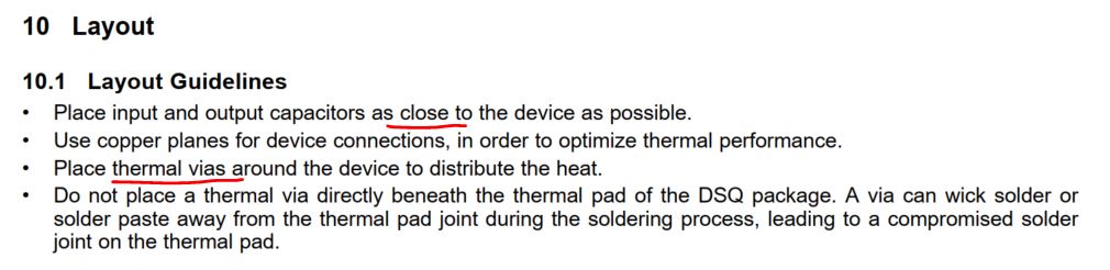
Something you need to be aware of:
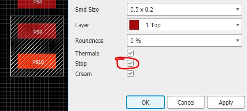
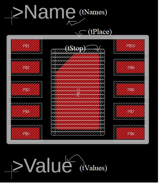
1. The distance btween the pads of TLV751 is only 0.4 mm, the 'tStop'
layer is too wide for this distance because the neighboring pads won't
have any solder mask in between.
Uncheck the 'stop' box in properties of the pad:
Re-draw the 'tstop' rectangles for each pad:
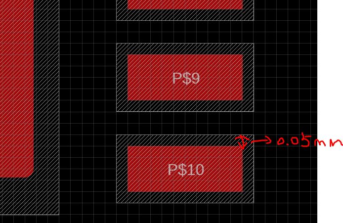
In its datasheet, the maximum 'tStop' can be used is 0.07 mm, we are using 0.05 mm so we are fine.
2. The thermal pad in the middle is grounded. You must do these things
to it to make it functioning: a. Use the polygon tool to draw the
thermal pad on the Top layer. b. Draw a 'tStop' polygon to wrap it up
so solder mask will not cover the pad. c. Put a real pad into the
center of the polygon thermal pad so it will be able to make
connections with others (GND). d. Make a indentation on the top-left
corner as the PIN1 indicator.
Draw a polygon top metal shape in the middle as the thermal pad. There
is no way to convert the polygon into a pin, so you have to create a
new pad (P$11), and drag it into the center of the polygon shape.
Finally, add the 'tName' and 'tValue' layers using the Text tool, and
add a 'tPlace' layer for the outline of the device (tPlace is the
silkscreen layer, which will be visible on the PCB).
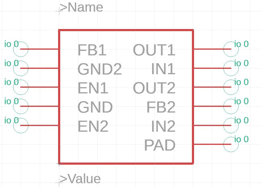
Follow the PCB tutorial to draw the symbol:
Make all the connections in the Device editing window:
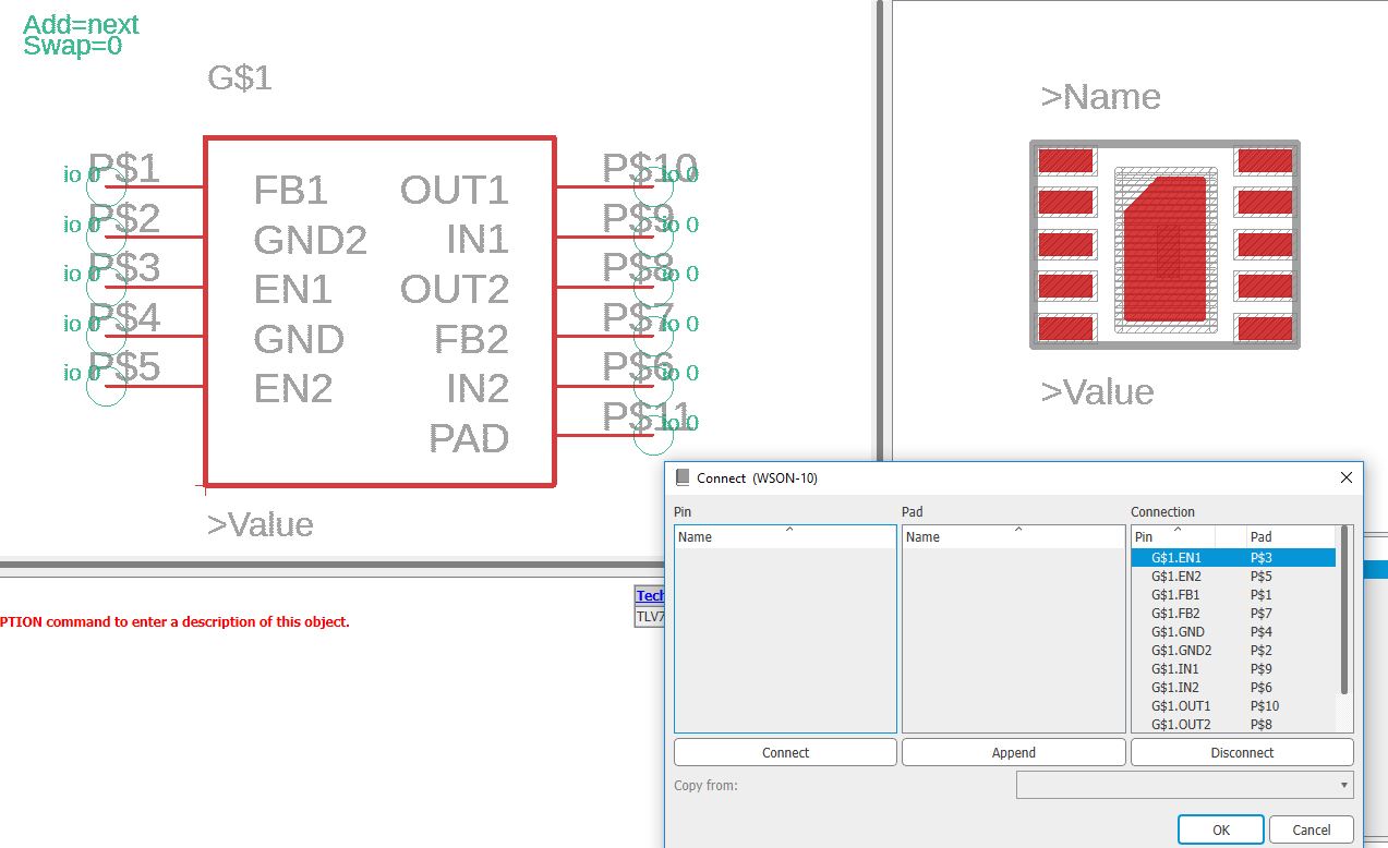
Do not forget to save it.
Now it is ready to use.
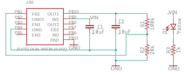
To add other capacitors, resistors, and LED (power indicator) to the schematic.
The SparkFun library has 0603 10 uF caps:
It also has the 0603 100 k, 20 k, and 1 k resistors:
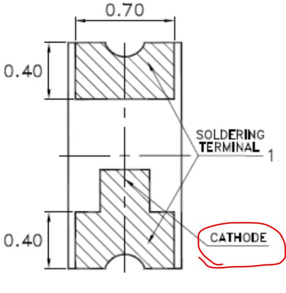
The 0603 Yellow color LED and the link of the LED I have ordered.
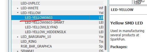
Ensure that you can tell which terminal is the cathode and which is the anode.
The current view of the schematic looks like this:
2. The ESP32-WROOM-32D module and the peripherals
The datasheet of the esp32-wroom-32d module can be found here.
The SparkFun library has the older WiFi module's device (ESP8266) but
not the new ESP32's. Yes, you can definitely create this device on your
own. We have done this a few times.
This time, let's find some resource online. There must be someone has
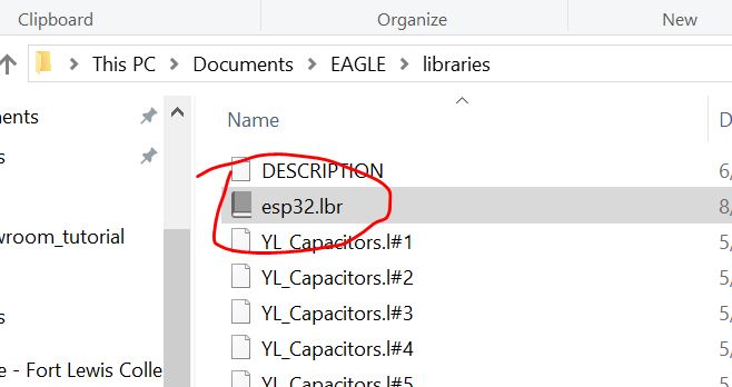
made it and put it in GitHub! A simple search gave me this result:
https://github.com/lpodkalicki/eagle-libraries/blob/master/ics/esp32.lbr
I downloaded the library file and put it in the library's folder. You can also download it from here.
so you can see and use it in Eagle PCB:
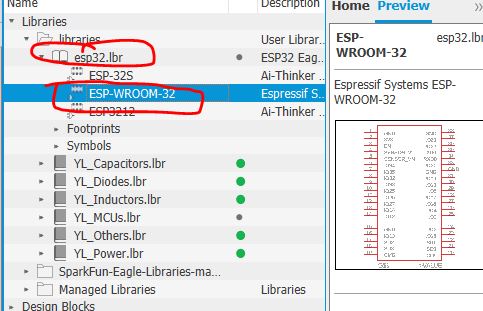
This saves us a lot of time.
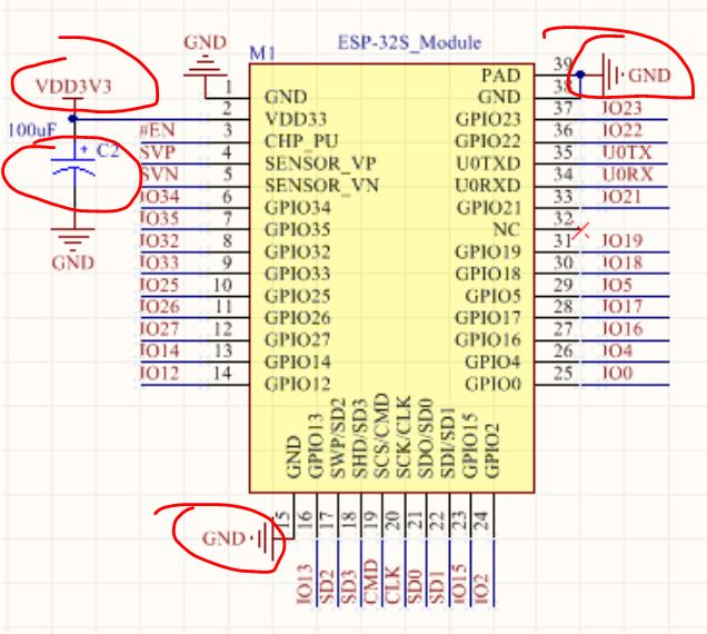
From ESP32-WROOM-32D schematic, we can find the necessary connections for the ESP32 module, the power supply, and the MPU chips.
Find the schematic/pinout of the ESP32-WROOM-32D module:
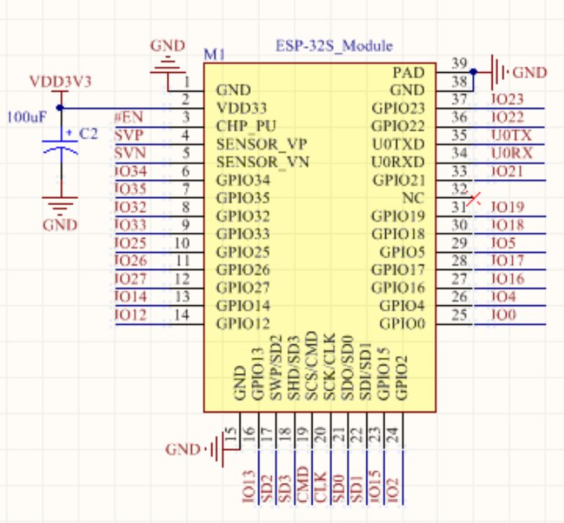
Make the following connections in your Eagle schematic: (the ESP32 module is available in the SparkFun library).
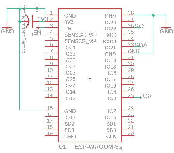
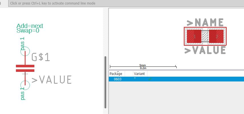
In the schematic above, the capacitor being used is a surface mount tantalum capacitor (package 1206). The link of the device is here, the datasheet is here.
Create a device in your capacitor library, use the SparkFun's 1206
package and the polarized symbol you created in the past (or use the
one in SparkFun's library).
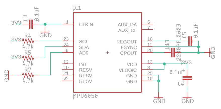
We can find the necessary connections of the MPU6050 chip from the schematic here. The library can be downloaded here, or from my server.
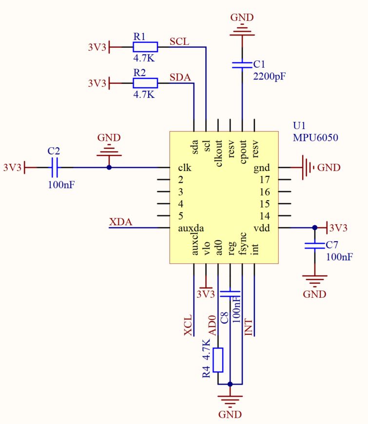
Let's make it in the schematic.
After placed all the available parts from the library, I found that the
2200pF 0603 capacitor is not available in there. Let's use a new method
to create this device in my 'YL_capacitors' library.
Double click the library in the Control Panel's window. Enter the
library's view, and click the 'footprint' option to 'import' the 0603
footprint from the SparkFun's Capacitor library.
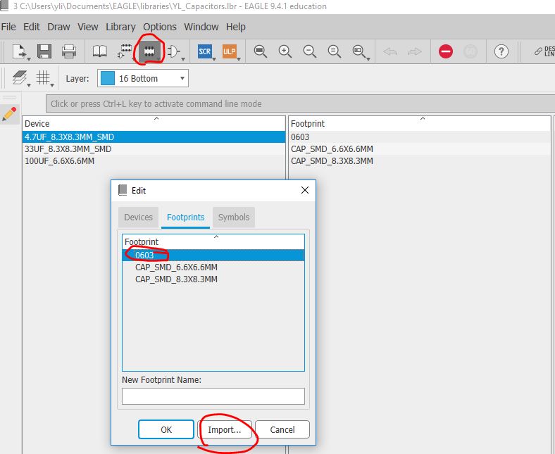
Do the same for the schematic. Import it from the SparkFun's library.
Then make a device out of the footprint and the schemtic you just imported.
Save it and use it in your schematic.
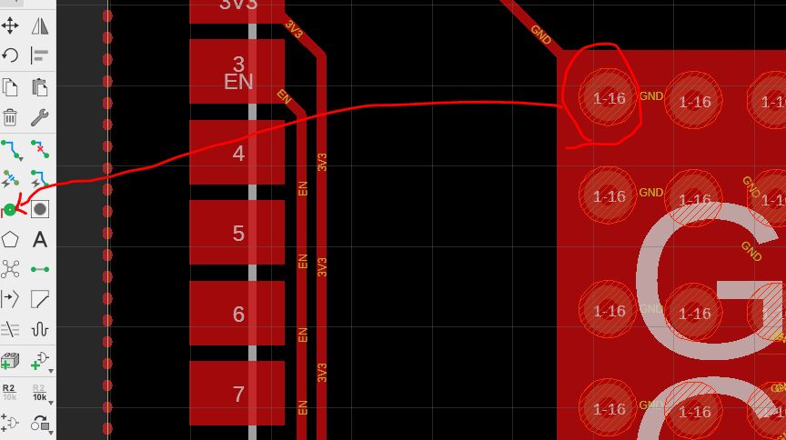
On the ESP32 module's schematic, the EN pin and the IO0 pin are pulled
up to VCC while it is operating. We are not going to let this board
programmable so we do not need the two pushbuttons used on the original
schematic.
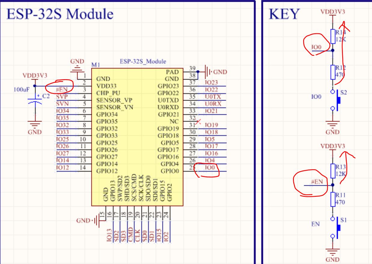
Also add a 2-pin connector to the board so you can solder the batteries anothe and cathode to it.
The pull up circuit is also added to the schematic.
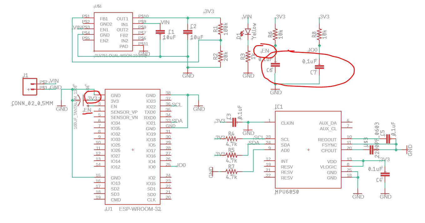
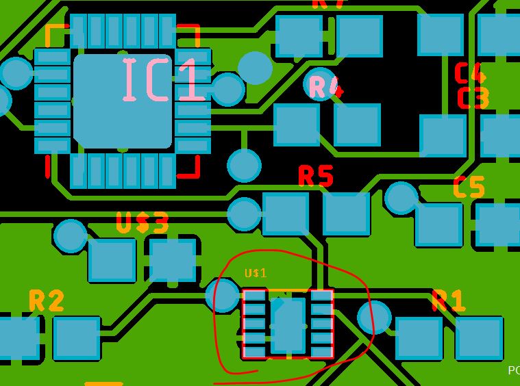
In the layout, try to keep the 10 uF capacitors of the power module
close to the power chip (this is always the rule for any DC power
modules anywhere).
Carefully arrange the layout of the board. I was able to reach a
footprint of 48.5 mm x 23.5 mm for the board. Keep in mind that if you
can put all the small parts on the back of the ESP32 module and use a
multi-layer PCB (more than 2 layers), you will be able to reduce the
size even more. In addition to that, there are smaller resistor
packages (visible by your naked eye) available. For example the 0402
footprint is a very popular package as well. However, I do not
recommend it here because it is a little too small for your tweezer and
for a course project like this. It's good to know all the possibilities
for this type of project.
The layout (you do not have to place the parts as dense as I did):
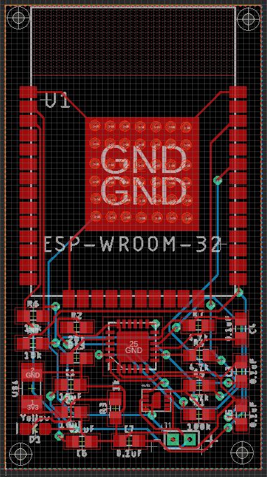
The pads array overlaps with
the GND plate are vias that transfer the heat to the bottom poured
coper. DRC may report errors as 'overlapping' but it is fine as long as
you know what you are doing.
These vias were added to the layout in the brd view, they were not added in the ESP's library.
Autoroute it and pour the coper: (pour copper to both sides of the board to dissipate heat generated from the DC-DC module).
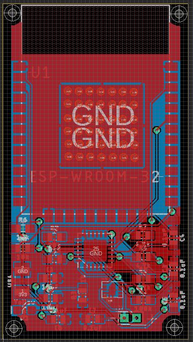
Create the gerber files. Check the silkscreen on https://onlinegerberviewer.azurewebsites.net/Viewer: (I found that I didn't have the '+ -' sign for the battery's connector and I added it after this checking.
Also, it's good to check the solder mask, to see if you 'tStop' keep
the solder mask away from your bare copper pads in your customized
parts.
Look at the footprint I created for TLV751, the metal pads are exposed
but not covered by the green color, which will be the solder mask.
Now, you are ready to order it on PCBWay.